CY7C67200
Document #: 38-08014 Rev. *G Page 43 of 78
Register Description
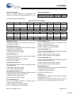
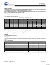
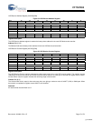
The GPIO 0 Direction register controls the direction of the GPIO data pins (input/output). The GPIO 0 Direction register controls
GPIO15 to GPIO0 while the GPIO 1 Direction register controls GPIO31 to GPIO19.
When any bit of this register is set to ‘1’, the corresponding GPIO data pin becomes an output. When any bit of this register is
set to ‘0’, the corresponding GPIO data pin becomes an input.
Reserved
All reserved bits must be written as ‘0’.
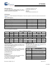
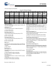
GPIO 1 Direction Register [0xC028] [R/W]
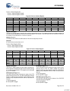
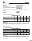
Figure 47. GPIO 1 Direction Register
Register Description
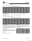
The GPIO 1 Direction register controls the direction of the GPIO data pins (input/output). The GPIO 0 Direction register controls
GPIO15 to GPIO0 while the GPIO 1 Direction register controls GPIO31 to GPIO19.
When any bit of this register is set to ‘1’, the corresponding GPIO data pin becomes an output. When any bit of this register is
set to ‘0’, the corresponding GPIO data pin becomes an input.
Reserved
All reserved bits must be written as ‘0’.
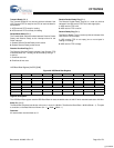
HSS Registers
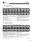
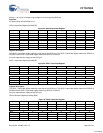
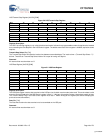
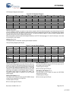
There are eight registers dedicated to HSS operation. Each of these registers are covered in this section and summarized in
Table 31.
Bit # 15 14 13 12 11 10 9 8
Field GPIO31 GPIO30 GPIO29 Reserved GPIO24
Read/Write R/W R/W R/W R/W R/W R/W R/W R/W
Default 0 0 0 0 0 0 0 0
Bit # 7 6 5 4 3 2 1 0
Field GPIO23 GPIO22 GPIO21 GPIO20 GPIO19 Reserved
Read/Write R/W R/W R/W R/W R/W R/W R/W R/W
Default 0 0 0 0 0 0 0 0
Table 31.HSS Registers
Register Name Address R/W
HSS Control Register 0xC070 R/W
HSS Baud Rate Register 0xC072 R/W
HSS Transmit Gap Register 0xC074 R/W
HSS Data Register 0xC076 R/W
HSS Receive Address Register 0xC078 R/W
HSS Receive Length Register 0xC07A R/W
HSS Transmit Address Register 0xC07C R/W
HSS Transmit Length Register 0xC07E R/W
[+] Feedback


