


CY7C67200
Document #: 38-08014 Rev. *G Page 49 of 78
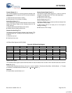
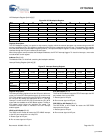
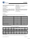
HPI Breakpoint Register [0x0140] [R]
Figure 56. HPI Breakpoint Register
Register Description
The HPI Breakpoint register is a special on-chip memory location, which the external processor can access using normal HPI
memory read/write cycles. This register is read-only by the CPU but is read/write by the HPI port. The contents of this register
have the same effect as the Breakpoint register [0xC014]. This special Breakpoint register is used by software debuggers which
interface through the HPI port instead of the serial port.
When the program counter matches the Breakpoint Address, the INT127 interrupt triggers. To clear this interrupt, a zero value
must be written to this register.
Address (Bits [15:0])
The Address field is a 16-bit field containing the breakpoint address.
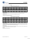
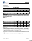
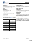
Interrupt Routing Register [0x0142] [R]
Figure 57. Interrupt Routing Register
Register Description
The Interrupt Routing register allows the HPI port to take over
some or all of the SIE interrupts that usually go to the on-chip
CPU. This register is read-only by the CPU but is read/write by
the HPI port. By setting the appropriate bit to ‘1’, the SIE
interrupt is routed to the HPI port to become the HPI_INTR
signal and also readable in the HPI Status register. The bits in
this register select where the interrupts are routed. The
individual interrupt enable is handled in the SIE interrupt
enable register.
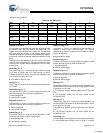
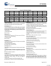
VBUS to HPI Enable (Bit 15)
The VBUS to HPI Enable bit routes the OTG VBUS interrupt
to the HPI port instead of the on-chip CPU.
1: Route signal to HPI port
0: Do not route signal to HPI port
ID to HPI Enable (Bit 14)
The ID to HPI Enable bit routes the OTG ID interrupt to the HPI
port instead of the on-chip CPU.
1: Route signal to HPI port
0: Do not route signal to HPI port
SOF/EOP2 to HPI Enable (Bit 13)
The SOF/EOP2 to HPI Enable bit routes the SOF/EOP2
interrupt to the HPI port.
1: Route signal to HPI port
0: Do not route signal to HPI port
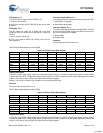
Bit # 15 14 13 12 11 10 9 8
Field Address...
Read/Write R R R R R R R R
Default 0 0 0 0 0 0 0 0
Bit # 7 6 5 4 3 2 1 0
Field ...Address
Read/Write R R R R R R R R
Default 0 0 0 0 0 0 0 0
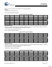
Bit # 15 14 13 12 11 10 9 8
Field
VBUS to HPI
Enable
ID to HPI
Enable
SOF/EOP2 to
HPI Enable
SOF/EOP2 to
CPU Enable
SOF/EOP1 to
HPI Enable
SOF/EOP1 to
CPU Enable
Reset2 to HPI
Enable
HPI Swap 1
Enable
Read/Write R R R R R R R R
Default 0 001010 0
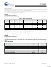
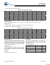
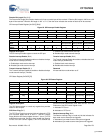
Bit # 7 6 5 4 3 2 1 0
Field
Resume2 to
HPI Enable
Resume1 to
HPI Enable
Reserved Done2 to HPI
Enable
Done1 to HPI
Enable
Reset1 to HPI
Enable
HPI Swap 0
Enable
Read/Write - - - - - - - -
Default 0 0 0 0 0 0 0 0
[+] Feedback