


CY7C67200
Document #: 38-08014 Rev. *G Page 42 of 78
Writing a 1 to any bit will output a high voltage on the corresponding GPIO pin.
Reserved
All reserved bits must be written as ‘0’.
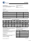
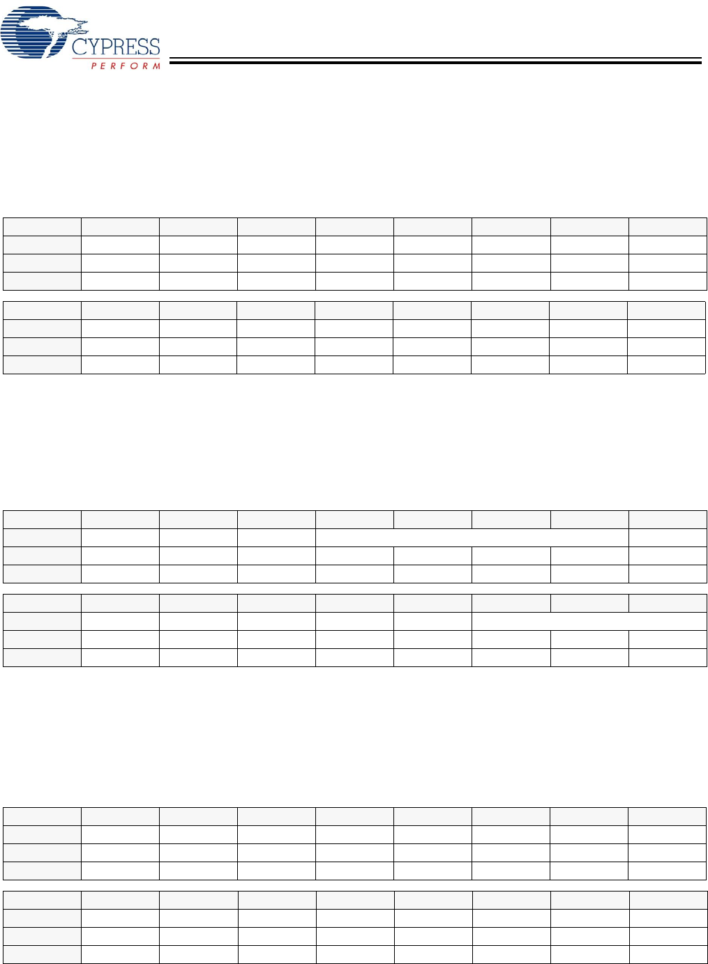
GPIO 0 Input Data Register [0xC020] [R]
Figure 44. GPIO 0 Input Data Register
Register Description
The GPIO 0 Input Data register reads the input data of the GPIO pins. The GPIO 0 Input Data register reads from GPIO15 to
GPIO0 while the GPIO 1 Input Data register reads from GPIO31 to GPIO19.
Every bit represents the voltage of that GPIO pin.
GPIO 1 Input Data Register [0xC026] [R]
Figure 45. GPIO 1 Input Data Register
Register Description
The GPIO 1 Input Data register reads the input data of the GPIO pins. The GPIO 0 Input Data register reads from GPIO15 to
GPIO0 while the GPIO 1 Input Data register reads from GPIO31 to GPIO19.
Every bit represents the voltage of that GPIO pin.
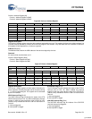
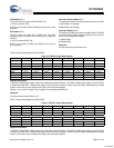
GPIO 0 Direction Register [0xC022] [R/W]
Figure 46. GPIO 0 Direction Register
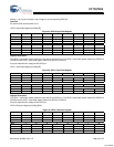
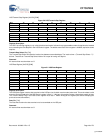
Bit # 15 14 13 12 11 10 9 8
Field GPIO15 GPIO14 GPIO13 GPIO12 GPIO11 GPIO10 GPIO9 GPIO8
Read/Write R R R R R R R R
Default 0 0 0 0 0 0 0 0
Bit # 7 6 5 4 3 2 1 0
Field GPIO7 GPIO6 GPIO5 GPIO4 GPIO3 GPIO2 GPIO1 GPIO0
Read/Write R R R R R R R R
Default 0 0 0 0 0 0 0 0
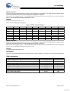
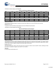
Bit # 15 14 13 12 11 10 9 8
Field GPIO31 GPIO30 GPIO29 Reserved GPIO24
Read/Write R R R - - - - R
Default 0 0 0 0 0 0 0 0
Bit # 7 6 5 4 3 2 1 0
Field GPIO23 GPIO22 GPIO21 GPIO20 GPIO19 Reserved
Read/Write R R R R R - - -
Default 0 0 0 0 0 0 0 0
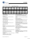
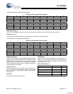
Bit # 15 14 13 12 11 10 9 8
Field GPIO15 GPIO14 GPIO13 GPIO12 GPIO11 GPIO10 GPIO9 GPIO8
Read/Write R/W R/W R/W R/W R/W R/W R/W R/W
Default 0 0 0 0 0 0 0 0
Bit # 7 6 5 4 3 2 1 0
Field GPIO7 GPIO6 GPIO5 GPIO4 GPIO3 GPIO2 GPIO1 GPIO0
Read/Write R/W R/W R/W R/W R/W R/W R/W R/W
Default 0 0 0 0 0 0 0 0
[+] Feedback