


CY7C67200
Document #: 38-08014 Rev. *G Page 60 of 78
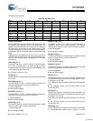
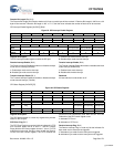
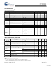
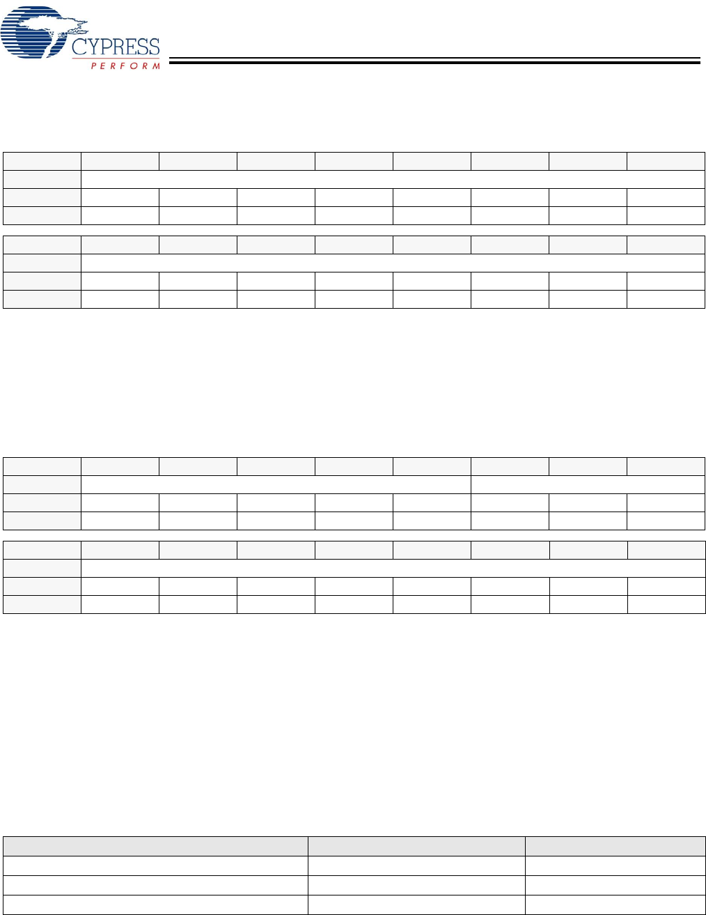
SPI Receive Address Register [0xC0DC [R/W]
Figure 71. SPI Receive Address Register
Register Description
The SPI Receive Address register is issued as the base address for the SPI Receive DMA.
Address (Bits [15:0])
The Address field sets the base address for the SPI receive DMA.
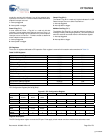
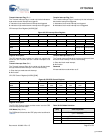
SPI Receive Count Register [0xC0DE] [R/W]
Figure 72. SPI Receive Count Register
Register Description
The SPI Receive Count register designates the block byte length for the SPI receive DMA transfer.
Count (Bits [10:0])
The Count field sets the count for the SPI receive DMA transfer.
Reserved
All reserved bits must be written as ‘0’.
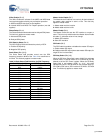
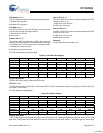
UART Registers
There are three registers dedicated to UART operation. Each of these registers is covered in this section and summarized in
Table 36.
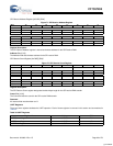
Bit # 15 14 13 12 11 10 9 8
Field Address...
Read/Write R/W R/W R/W R/W R/W R/W R/W R/W
Default 0 0 0 0 0 0 0 0
Bit # 7 6 5 4 3 2 1 0
Field ...Address
Read/Write R/W R/W R/W R/W R/W R/W R/W R/W
Default 0 0 0 0 0 0 0 0
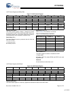
Bit # 15 14 13 12 11 10 9 8
Field Reserved Count...
Read/Write - - - - - R/W R/W R/W
Default 0 0 0 0 0 0 0 0
Bit # 7 6 5 4 3 2 1 0
Field ...Count
Read/Write R/W R/W R/W R/W R/W R/W R/W R/W
Default 0 0 0 0 0 0 0 0
Table 36.UART Registers
Register Name Address R/W
UART Control Register 0xC0E0 R/W
UART Status Register 0xC0E2 R
UART Data Register 0xC0E4 R/W
[+] Feedback