


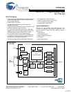
CY7C67200
Document #: 38-08014 Rev. *G Page 5 of 78
Host Port Interface (HPI)
EZ-OTG has an HPI interface. The HPI interface provides
DMA access to the EZ-OTG internal memory by an external
host, plus a bidirectional mailbox register for supporting
high-level communication protocols. This port is designed to
be the primary high-speed connection to a host processor.
Complete control of EZ-OTG can be accomplished through
this interface via an extensible API and communication
protocol. Other than the hardware communication protocols, a
host processor has identical control over EZ-Host whether
connecting to the HPI or HSS port. The HPI interface is
exposed through GPIO pins.
Note It should be noted that for up to 3 ms after BIOS starts
executing, GPIO[24:19] and GPIO[15:8] will be driven as
outputs for a test mode. If these pins need to be used as inputs,
a series resistor is required (10 ohm to 48 ohm is recom-
mended). Refer to BIOS documentation for addition details.
See section “Reset Pin” on page 9.
HPI Features
• 16-bit data bus interface
• 16 MB/s throughput
• Auto-increment of address pointer for fast block mode
transfers
• Direct memory access (DMA) to internal memory
• Bidirectional Mailbox register
• Byte Swapping
• Complete access to internal memory
• Complete control of SIEs through HPI
• Dedicated HPI Status register
HPI Pins
The two HPI address pins are used to address one of four
possible HPI port registers as shown in Table 10 below.
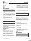
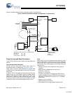
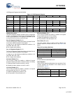
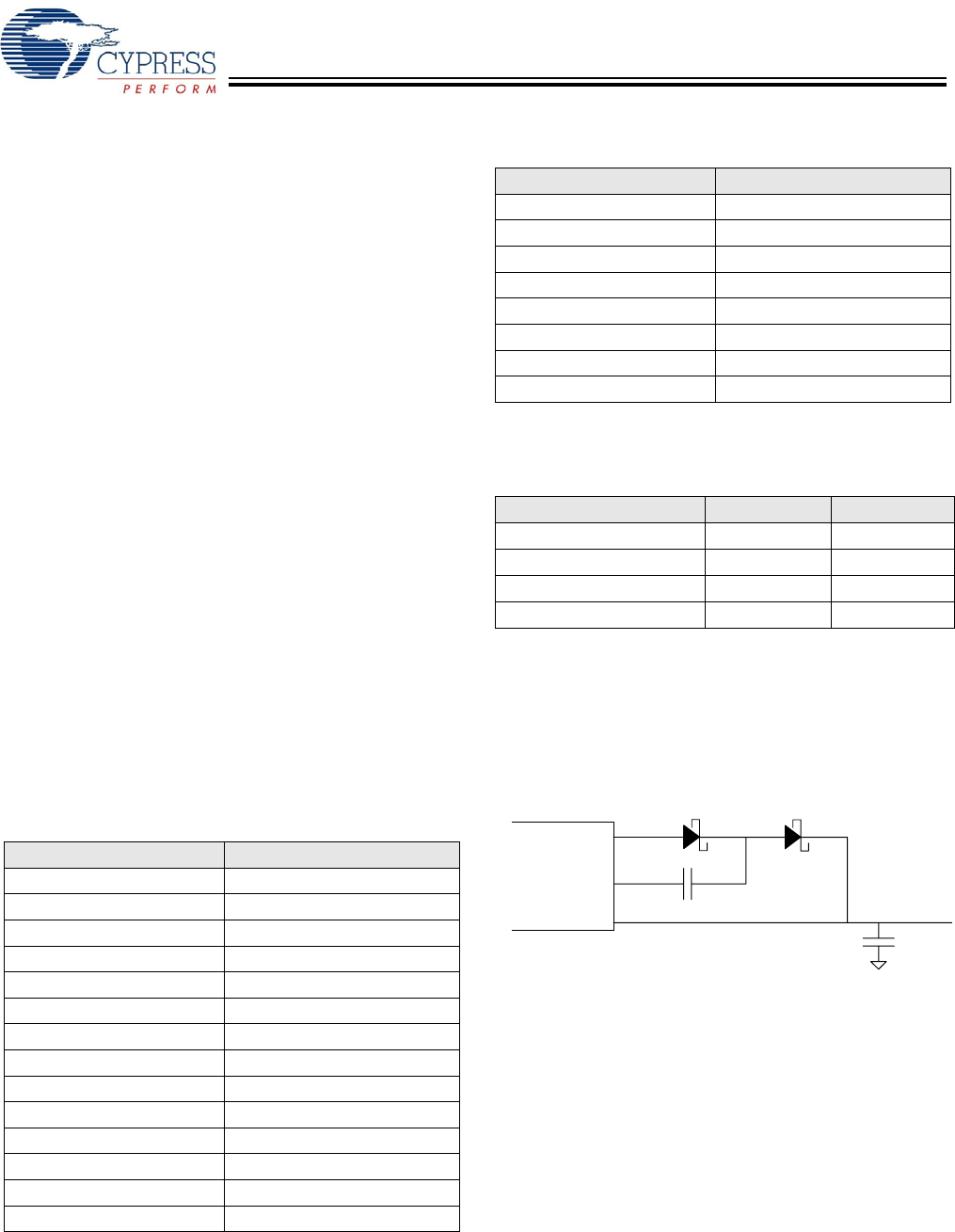
Charge Pump Interface
VBUS for the USB On-The-Go (OTG) port can be produced by
EZ-OTG using its built-in charge pump and some external
components. The circuit connections should look similar to
Figure 1 below.
Component details:
• D1 and D2: Schottky diodes with a current rating greater
than 60 mA.
• C1: Ceramic capacitor with a capacitance of 0.1 µF.
• C2: Capacitor value must be no more that 6.5 µF since that
is the maximum capacitance allowed by the USB OTG
specification for a dual-role device. The minimum value of
C2 is 1 µF. There are no restrictions on the type of capacitor
for C2.
If the VBUS charge pump circuit is not to be used,
CSWITCHA, CSWITCHB, and OTGVBUS can be left uncon-
nected.
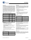
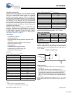
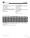
Table 9. HPI Interface Pins
[1, 2]
Pin Name Pin Number
INT H4
nRD G4
nWR H5
nCS G5
A1 H6
A0 F5
D15 F6
D14 E4
D13 E5
D12 E6
D11 D4
D10 D5
D9 C6
D8 C5
Notes
1. HPI_INT is for the Outgoing Mailbox Interrupt.
2. HPI strobes are negative logic sampled on rising edge.
D7 B5
D6 B4
D5 C4
D4 B3
D3 A3
D2 C3
D1 A2
D0 B2
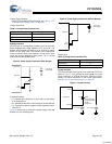
Table 10.HPI Addressing
HPI A[1:0] A1 A0
HPI Data 0 0
HPI Mailbox 0 1
HPI Address 1 0
HPI Status 1 1
Figure 1. Charge Pump
Table 9. HPI Interface Pins
[1, 2]
(continued)
Pin Name Pin Number
CSWITCHA
CY7C67200
CSWITCHB
OTGVBUS
D1
D2
C1
C2
VBUS
[+] Feedback