


CY7C67200
Document #: 38-08014 Rev. *G Page 66 of 78
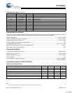
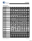
DC Characteristics
Notes
6. All tests were conducted with Charge pump off.
7. I
CC
and I
CCB
values are the same regardless of USB host or peripheral configuration.
8. There is no appreciable difference in I
CC
and I
CCB
values when only one transceiver is powered.
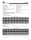
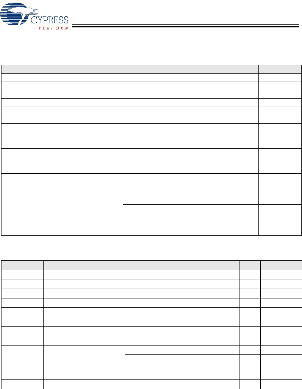
Table 40.DC Characteristics
[6]
Parameter Description Conditions Min. Typ. Max. Unit
V
CC
, AV
CC
Supply Voltage 3.0 3.3 3.6 V
BoosV
CC
Supply Voltage 2.7 3.6 V
V
IH
Input HIGH Voltage 2.0 5.5 V
V
IL
Input LOW Voltage 0.8 V
I
I
Input Leakage Current 0< V
IN
< V
CC
–10.0 +10.0 µA
V
OH
Output Voltage HIGH I
OUT
= 4 mA 2.4 V
V
OL
Output LOW Voltage I
OUT
= –4 mA 0.4 V
I
OH
Output Current HIGH 4mA
I
OL
Output Current LOW 4mA
C
IN
Input Pin Capacitance Except D+/D– 10 pF
D+/D– 15 pF
V
HYS
Hysteresis on nReset Pin 250 mV
I
CC
[7, 8]
Supply Current 2 transceivers powered 80 100 mA
I
CCB
[7, 8]
Supply Current with Booster Enabled 2 transceivers powered 135 180 mA
I
SLEEP
Sleep Current USB Peripheral: includes 1.5K
internal pull up
210 500 µA
Without 1.5K internal pull up 5 30 µA
I
SLEEPB
Sleep Current with Booster Enabled USB Peripheral: includes 1.5K
internal pull up
210 500 µA
Without 1.5K internal pull up 5 30 µA
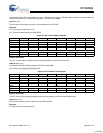
Table 41.DC Characteristics: Charge Pump
Parameter Description Conditions Min. Typ. Max. Unit
V
A_VBUS_OUT
Regulated OTGVBUS Voltage 8 mA< I
LOAD
< 10 mA 4.4 5.25 V
T
A_VBUS_RISE
V
BUS
Rise Time I
LOAD
= 10 mA 100 ms
I
A_VBUS_OUT
Maximum Load Current 8 10 mA
C
DRD_VBUS
OUTVBUS Bypass Capacitance 4.4V< V
BUS
< 5.25V 1.0 6.5 pF
V
A_VBUS_LKG
OTGVBUS Leakage Voltage OTGVBUS not driven 200 mV
V
DRD_DATA_LKG
Dataline Leakage Voltage 342 mV
I
CHARGE
Charge Pump Current Draw I
LOAD
= 8 mA 20 20 mA
I
LOAD
= 0 mA 0 1 mA
I
CHARGEB
Charge Pump Current Draw with
Booster Active
I
LOAD
= 8 mA 30 45 mA
I
LOAD
= 0 mA 0 5 mA
I
B_DSCHG_IN
B-Device (SRP Capable)
Discharge Current
0V< V
BUS
< 5.25V 8 mA
V
A_VBUS_VALID
A-Device VBUS Valid 4.4 V
[+] Feedback