CY7C67200
Document #: 38-08014 Rev. *G Page 53 of 78
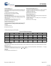
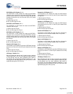
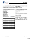
mode this read only bit indicates if any of the endpoint inter-
rupts occurs on Device 2. Firmware needs to determine which
endpoint interrupt occurred.
1: Interrupt triggered
0: Interrupt did not trigger
Done1 Flag (Bit 2)
In host mode the Done 1 Flag bit is a read-only bit that
indicates if a host packet done interrupt occurs on Host 1. In
device mode this read-only bit indicates if any of the endpoint
interrupts occurs on Device 1. Firmware needs to determine
which endpoint interrupt occurred.
1: Interrupt triggered
0: Interrupt did not trigger
Reset1 Flag (Bit 1)
The Reset1 Flag bit is a read-only bit that indicates if a USB
Reset interrupt occurs on either Host/Device 1.
1: Interrupt triggered
0: Interrupt did not trigger
Mailbox Out Flag (Bit 0)
The Mailbox Out Flag bit is a read-only bit that indicates if a
message is ready in the outgoing mailbox. This interrupt clears
when the external host reads from the HPI Mailbox register.
1: Interrupt triggered
0: Interrupt did not trigger
SPI Registers
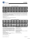
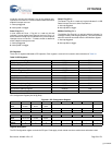
There are 12 registers dedicated to SPI operation. Each register is covered in this section and summarized in Table 3 3.
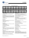
SPI Configuration Register [0xC0C8] [R/W]
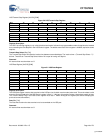
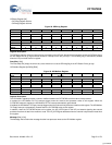
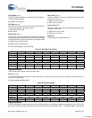
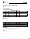
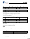
Figure 61. SPI Configuration Register
Register Description
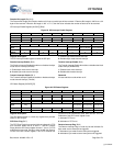
The SPI Configuration register controls the SPI port. Fields apply to both master and slave mode unless otherwise noted.
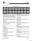
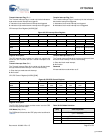
Table 33.SPI Registers
Register Name Address R/W
SPI Configuration Register 0xC0C8 R/W
SPI Control Register 0xC0CA R/W
SPI Interrupt Enable Register 0xC0CC R/W
SPI Status Register 0xC0CE R
SPI Interrupt Clear Register 0xC0D0 W
SPI CRC Control Register 0xC0D2 R/W
SPI CRC Value 0xC0D4 R/W
SPI Data Register 0xC0D6 R/W
SPI Transmit Address Register 0xC0D8 R/W
SPI Transmit Count Register 0xC0DA R/W
SPI Receive Address Register 0xC0DC R/W
SPI Receive Count Register 0xC0DE R/W
Bit # 15 14 13 12 11 10 9 8
Field
3Wire
Enable
Phase
Select
SCK Polarity
Select
Scale Select Reserved
Read/Write R/W R/W R/W R/W R/W R/W R/W -
Default 1 0 0 0 0 0 0 0
Bit # 7 6 5 4 3 2 1 0
Field
Master
Active Enable
Master
Enable
SS
Enable
SS Delay Select
Read/Write R R/W R/W R/W R/W R/W R/W R/W
Default 0 0 0 1 1 1 1 1
[+] Feedback


