


L2002 Inverter
Appendix B
B–41
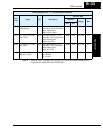
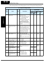
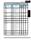
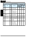
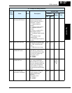
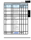
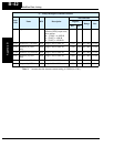
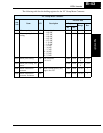
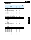
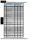
C081 O input span calibration R/W Scale factor between the
external frequency command
on terminals L – O (voltage
input) and the frequency
output, range is 0.0 to 200.0%
1141h 04417 0 to 2000 0.1 %
C082 OI input span calibra-
tion
R/W Scale factor between the
external frequency command
on terminals L – OI (current
input) and the frequency
output, range is 0.0 to 200.0%
1142h 04418 0 to 2000 0.1 %
C085 Thermistor input tuning R/W Range is 0.0 to 200.0% 1144h 04420 0 to 2000 0.1 %
C086 [AM] terminal offset
tuning
R/W Range is 0.0 to 10.0V 1145h 04421 0 to 100 0.1 V
C091 Debug mode enable R Displays debug parameters.
Two option codes:
00...Disable
01...Enable
1148h 04424 0, 1 —
C101 Up/Down memory
mode
selection
R/W Controls speed setpoint for
the inverter after power cycle.
Two option codes:
00...Clear last frequency
(return to default frequency
F001)
01...Keep last frequency
adjusted by UP/DWN
1149h 04425 0, 1 —
C102 Reset selection R/W Determines response to Reset
input [RST].
Three option codes:
00...Cancel trip state at input
signal ON transition, stops
inverter if in Run Mode
01...Cancel trip state at signal
OFF transition, stops inverter
if in Run Mode
02...Cancel trip state at input
signal ON transition, no effect
if in Run Mode
114Ah 04426 0, 1, 2 —
C141 Input A select for logic
output
R/W
See
“Output Logic and
Timing” on page 3–61
1150h 04432 0, 1, 2, 3,
4, 5, 6, 7,
8, 9
—
C142 Input B select for logic
output
R/W 1151h 04433
“C” Group Intelligent Terminal Functions
Func.
Code
Name R/W Description
Network Data
Register
Range Res.
hex dec.