


Intel
®
IXP45X and Intel
®
IXP46X Product Line of Network Processors—General Hardware
Design Considerations
Intel
®
IXP45X and Intel
®
IXP46X Product Line of Network Processors
HDD February 2007
18 Document Number: 305261; Revision: 004
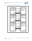
3.2 DDR-266 SDRAM Interface
The IXP45X/IXP46X network processors support unbuffered, DDR-266 SDRAM
technology, capable of addressing two memory banks (one bank per CS). Each bank
can be configured to support 32/64/128/256/512-Mbyte for a total combined memory
support of 1 Gbyte.
The device supports non-ECC and ECC for error correction, which can be enable or
disable by software as required. Banks have a bus width of 32 bits for non ECC or
40 bits for ECC enable (32-bit data + 8-bit ECC).
For a complete feature list, see the Intel
®
IXP45X and Intel
®
IXP46X Product Line of
Network Processors Datasheet.
General DDR SDRAM routing guidelines can be found in Section 7.1.7, “Routing
Guidelines” on page 88. For more detailed information, see the PC266 DDR SDRAM
specification.
3.2.1 Signal Interface
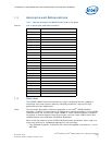
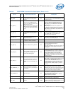
Table 3. Soft Fusible Features
Name Description
PCI The complete bus must be enabled or disable.
HSS0/1 Can only be disable as a pair.
UTOPIA
If enabling UTOPIA, MACs on NPE A are disabled.
If enabling MACs on NPE A, UTOPIA are disabled.
ETHERNET
Can Enable either MII MACs or SMII MACs, but not both at the same time. Enable of MACs
can be separately done per each NPE.
USB Host Each USB can be Enable separately.
USB Device Each USB can be Enable separately.
DDR ECC DDR can be disabled separately form the rest of the DDR interface.
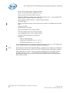
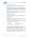
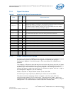
Table 4. DDR SDRAM Interface Pin Description (Sheet 1 of 2)
Name
Input
Outpu
t
Device-Pin Connection
VTT
Terminatio
n
Description
DDRI_CK[2:0] O
Connect a pair of differential clock
signals to every device; When
using both banks, daisy chain
devices with same data bit
sequence.
No
DDR SDRAM Clock Out — Provides the positive
differential clocks to the external SDRAM
memory subsystem.
DDRI_CK_N[2:0] O Same as above No
DDR SDRAM Clock Out — Provides the
negative differential clocks to the external
SDRAM memory subsystem.
DDRI_CS_N[1:0] O
Use the same CS to control 32-bit
data + 8-bit ECC, per bank
Yes
Chip Select — Must be asserted for all
transactions to the DDR SDRAM device. One
per bank.
DDRI_RAS_N O
The RAS signal must be connected
to each device in a daisy chain
manner
Yes
Row Address Strobe — Indicates that the
current address on DDRI_MA[13:0] is the row.
DDRI_CAS_N O
The CAS signal must be connected
to each device in a daisy chain
manner
Yes
Column Address Strobe — Indicates that the
current address on DDRI_MA[13:0] is the
column.