


Intel
®
IXP45X and Intel
®
IXP46X Product Line of Network Processors—Category
Intel
®
IXP45X and Intel
®
IXP46X Product Line of Network Processors
HDD February 2007
84 Document Number: 305261, Revision: 004
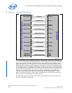
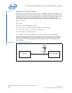
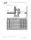
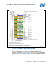
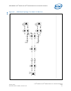
7.1.3 Printed Circuit Board Layer Stackup
The layer stackup used for the IXDP465 platform x16 Processor Module is shown in
Figure 35 on page 85. The example is for a 12-layer, printed circuit board with eight
signal layers and four plane layers.
• Layers 5 and 8 are used as digital ground planes
• Layers 2 and 11 are used as split planes for the different voltage references (3.3 V
and 2.5 V).
Details on the voltage reference layout are available in the CAD database or Gerber
files database for the IXDP465 platform x16 Processor Module.
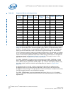
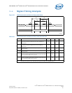
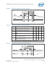
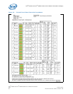
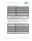
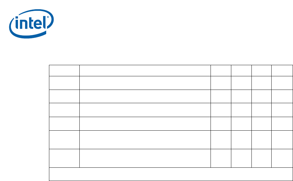
Table 32. DDR-Clock-to-DQS-Write Timing Parameters
Symbol Parameter Min Max Units Notes
T
1
IXP45X/IXP46X network processors output valid for
DDRI_DQS prior to the transition of DDR_M_CLK
1.4 ns 1
T
2
IXP45X/IXP46X network processors output hold time for
DDRI_DQS after the transition of DDR_M_CLK
1.0 ns 1
T
3
Required write command to DQS latching transition at
DDR memory device (early transition)
1.875 ns 1
T
4
Required write command to DQS latching transition at
DDR memory device (late transition)
1.875 ns 1
T
5
Allowable difference between IXP45X/IXP46X network
processors DDR_M_CLK output and first DQS transition
(early transition)
0.475 ns 1
T
6
Allowable difference between IXP45X/IXP46X network
processors DDR_M_CLK output and first DQS transition
(late transition)
0.875 ns 1
Notes:
1. DDR_M_CLK represents the combined clock signal for DDR_CK and DDR_CK_N.