


Intel
®
IXP45X and Intel
®
IXP46X Product Line of Network Processors
February 2007 HDD
Document Number: 305261; Revision: 004 27
General Hardware Design Considerations—Intel
®
IXP45X and Intel
®
IXP46X Product Line of
Network Processors
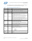
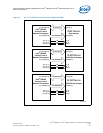
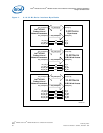
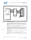
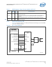
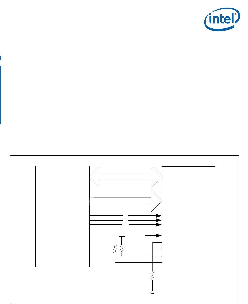
3.3.6 Flash Interface
Figure 5 illustrates how a boot ROM is connected to the expansion bus. The flash (ROM)
used in the block diagram is the Intel StrataFlash
®
memory device TE28F256J3D —
32-Mbyte, 16-bit, flash in the 56-TSOP package. The Intel StrataFlash memory
TE28F256J3D is part of the 0.13-micron, 3.3-V Intel StrataFlash memory.
The E28F256J3D supports common flash interface (CFI). For information on migrating
from J3 to J3D Intel StrataFlash memory, see the Intel StrataFlash
®
Memory J3 to
Intel
®
Embedded Flash Memory (J3 v.D) Conversion Guide - Application Note 835
(document 308555).
For information on migrating from J3 to P30 Intel StrataFlash memory, see the
Migration Guide for Intel StrataFlash
®
Memory (J3) to Intel StrataFlash
®
Embedded
Memory (P30 and P33) - Application Note 835 (document 308555).
The example in Figure 5 shows a 16-bit flash memory device connected to the IXP45X/
IXP46X network processors. Boot-strapping is required in the address bus, both
EX_ADDR[0] and EX_ADDR[7] need external, 4.7-KΩ pull-down resistors (not shown
on diagram). The pull-down resistors sets Bits 0 and 7 low in the Configuration Register
0. This in turn sets the processor into a 16-bit-mode access.
Figure 5. Flash Interface Example
E
X
_
A
D
D
R
[
2
4
:
0
]
EX_DATA[15:0]
16-Bit Device
16-Bit-Word Access
Intel
®
Flash
CS
OE
WR
EX_ADDR[24:0]
EX_DATA[31:0]
EX_CS_N
EX_RD_N
EX_WR_N
CE0
OE_N
WR_N
DATA[15:0]
ADDR[24:0]
CE1
CE2
RP_N
BYTE_N
VPEN_N
RST#
3.3 V
Intel
®
IXP46X
Product Line of
Network Processors
B4097-003
4.7 KΩ 4.7 KΩ
4.7 KΩ