


Intel
®
IXP45X and Intel
®
IXP46X Product Line of Network Processors
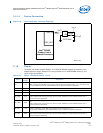
February 2007 HDD
Document Number: 305261; Revision: 004 63
General Layout and Routing Guide—Intel
®
IXP45X and Intel
®
IXP46X Product Line of Network
Processors
5.0 General Layout and Routing Guide
5.1 Overview
This chapter provides routing and layout guides for hardware and systems based on the
Intel
®
IXP45X and Intel
®
IXP46X Product Line of Network Processors.
The high-speed clocking required when designing with the processors requires special
attention to signal integrity. In fact, it is highly recommended that the board design be
simulated to determine optimum layout for signal integrity. The information in this
chapter provides guidelines to aid designers with board layout. In cases where it is too
difficult to follow a design rule, engineering judgment must be used.
5.2 General Layout Guidelines
The layout guidelines recommended in this section are based on experience and
knowledge gained from previous designs. Layer stacking varies, depending on design
complexity, however following standard rules helps minimize potential problems
dealing with signal integrity.
The following are well know documented recommendations that helps route a
functional board:
• Providing enough routing layers to comply with minimum and maximum timing
requirements of the IXP45X/IXP46X network processors and other components.
• Connectors, and mounting holes must be placed in a ways that will not interfere
with basic design guidelines in this document.
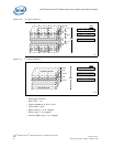
• Provide uniform impedance throughout the board, specially for high speed areas
such us clocking, DDR-SDRAM, PCI, device bus, etc.
• Place analog, high-voltage, power supply, low-speed, and high-speed devices in
different sections of the board.
• Decoupling capacitors must be placed next to power pins.
• Series termination resistors must be placed close to the source.
• Analog and digital sections of the board must be physically isolated from each
other. No common ground, power planes, and signal traces are allowed to cross-
isolation zones. Use appropriately sized PCB traces for larger enough to handle
peak current. Keep away from high-speed digital signals.
• Keep stubs as short as possible (preferably, the electrical length of the stub less
than half of the length of the rise time of signal).
• All critical signals should be routed before all other non-critical signals.
• Do not route signals close to the edge of the board, power or ground planes. Route
signal at least 50 to 100 mils away from the edge of the plane.
• Try to match buses to the same trace length and keep them in groups adjacent to
each other, away from other signals.
• Route processor address, data and control signals using a “daisy-chain” topology.
• Minimize number of vias and corners on all high speed signals.
• Do not route under crystals or clock oscillators, clock synthesizers, or magnetic
devices (ferrites, toroids).
• Maintain trace spacing consistent between differential pairs and match trace length.
• Keep differential signals away from long and parallel, high-speed paths, such as
clock signals and data strobe signals.