


Intel
®
IXP45X and Intel
®
IXP46X Product Line of Network Processors
February 2007 HDD
Document Number: 305261; Revision: 004 19
General Hardware Design Considerations—Intel
®
IXP45X and Intel
®
IXP46X Product Line of
Network Processors
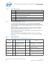
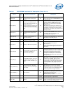
DDRI_WE_N O
The WE signal must be connected
to each device in a daisy chain
manner
Yes
Write Strobe — Defines whether or not the
current operation by the DDR SDRAM is to be
a read or a write.
DDRI_DM[4:0] O
Connect to each DM device pin.
For the 8-bit devices connect one
DM signal per device.
For the 16-bit devices connect two
DM signal per device (depending
on how many data bits are being
used).
Yes
Data Bus Mask — Controls the DDR SDRAM
data input buffers. Asserting DDRI_WE_N
causes the data on DDRI_DQ[31:0] and
DDRI_CB[7:0] to be written into the DDR
SDRAM devices.
DDRI_DM[4:0] controls this operation on a
per-byte basis. DDRI_DM[3:0] are intended to
correspond to each byte of a word of data.
DDRI_DM[4] is intended to be utilized for the
ECC byte of data.
DDRI_BA[1:0] O
The BA signals must be connected
to each device in a daisy chain
manner.
Yes
DDR SDRAM Bank Selects — Controls which of
the internal DDR SDRAM banks to read or
write. DDRI_BA[1:0] are used for all
technology types supported.
DDRI_MA[13:0] O
All address signals need to be
connected to each device in a
daisy chain manner.
Yes
Address bits 13 through 0 — Indicates the row
or column to access depending on the state of
DDRI_RAS_N and DDRI_CAS_N.
DDRI_DQ[31:0] I/O
Need to be connected in parallel
to achieve a 32-bit bus width.
Yes Data Bus — 32-bit wide data bus.
DDRI_CB[7:0] I/O Connect to ECC memory devices. Yes
ECC Bus — Eight-bit error correction code
which accompanies the data on
DDRI_DQ[31:0].
When ECC is disabled and not being used in a
system design, these signals can be left un-
connected.
DDRI_DQS[4:0] I/O
Connect DQS[3:0] to devices with
data signals and DQS[4] to
devices with ECC signals.
Yes
Data Strobes Differential — Strobes that
accompany the data to be read or written from
the DDR SDRAM devices. Data is sampled on
the negative and positive edges of these
strobes. DDRI_DQS[3:0] are intended to
correspond to each byte of a word of data.
DDRI_DQS4] is intended to be utilized for the
ECC byte of data.
DDRI_CKE[1:0] O
Use one CKE per bank, never mix
the CKE on the same bank. Use
CKE[0] for bank0 and CKE[1] for
bank1
Yes
Clock enables — One clock after
DDRI_CKE[1:0] is de-asserted, data is latched
on DQ[31:0] and DDRI_CB[7:0]. Burst
counters within DDR SDRAM device are not
incremented. De-asserting this signal places
the DDR SDRAM in self-refresh mode. For
normal operation, DDRI_CKE[1:0] must be
asserted.
DDRI_RCVENOUT_N O
Connect RCVEOUT to RCVENIN
and follow note on pin description
in this table.
No
RECEIVE ENABLE OUT must be connected to
DDRI_RCVENIN_N signal of the IXP45X/
IXP46X product line and the propagation delay
of the trace length must be matched to the
clock trace plus the average DQ Traces.
DDRI_RCVENIN_N I Same as above No
RECEIVE ENABLE IN provides delay
information for enabling the input receivers
and must be connected to the
DDRI_RCVENOUT_N signal
of the IXP45X/
IXP46X network processors.
DDRI_RCOMP O Tied off to a resistor
Tied off to a
resistor
20 Ohm Resistor connected to ground used for
process/temperature adjustments.
DDRI_VREF I VCCM/2 VCCM/2
DDR SDRAM Voltage Reference — is used to
supply the reference voltage to the differential
inputs of the memory controller pins.
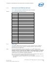
Table 4. DDR SDRAM Interface Pin Description (Sheet 2 of 2)
Name
Input
Outpu
t
Device-Pin Connection
VTT
Terminatio
n
Description