


Intel
®
IXP45X and Intel
®
IXP46X Product Line of Network Processors—Category
Intel
®
IXP45X and Intel
®
IXP46X Product Line of Network Processors
HDD February 2007
64 Document Number: 305261; Revision: 004
• Do not place high-frequency oscillators and switching network devices close to
sensitive analog circuits.
• Arrange the board so that return currents for high-speed traces never must jump
between planes. Restrict traces to remain on either side of whichever ground plane
they start out nearest. This allows the use of naturally grouped horizontal and
vertical routing layers.
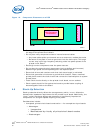
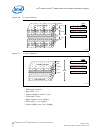
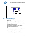
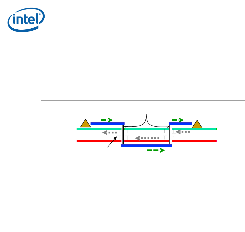
If signals change between layers, the reference voltage changes, as shown in
Figure 22. This creates discontinuity in the path of the signal.
The design in Figure 22, routes a signal on the top layer, close to GND plane, and
provides a very good return current path. The signal then is routed to the bottom layer,
close to the PWR plane, such that the return currents flows to the ground plane through
bypass caps. Hence the path for the return currents is less inductive than in the
previous case when the signal is routed on the top layer.
5.2.1 General Component Spacing
• Do not place components within 125 mils to the edge of the printed circuit board.
For exact dimensions consult your manufacturing vendor.
• Keep a minimum spacing between via and the solder pad edges > 25mil.
• Position devices that interface with each other close to one another to minimize
trace lengths.
Figure 22. Signal Changing Reference Planes
B2269-01
GND
PWR
Driver
Receiver
Trace
VIAs
Signal
Return Current
Signal
Signal
ByPass Caps