


Intel
®
IXP45X and Intel
®
IXP46X Product Line of Network Processors
February 2007 HDD
Document Number: 305261, Revision: 004 5
Contents—Intel
®
IXP45X and Intel
®
IXP46X Product Line of Network Processors
7.1.7.1 Clock Group ............................................................................. 88
7.1.7.2 Data, Command, and Control Groups........................................... 89
7.2 Simulation Results............................................................................................. 90
7.2.1 Clock Group........................................................................................... 90
7.2.2 Data Group ........................................................................................... 92
7.2.3 Control Group ........................................................................................ 98
7.2.4 Command Group.................................................................................. 100
7.2.5 RCVENIN and RCVENOUT ...................................................................... 105
Figures
1Intel
®
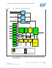
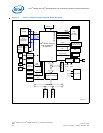
IXP465 Component Block Diagram.................................................................... 13
2Intel
®
IXP465 Example System Block Diagram ............................................................ 16
3 8/16/32-Bit Device Interface: No Byte-Enable.............................................................. 25
4 8/16/32-Bit Device Interface: Byte Enable................................................................... 26
5 Flash Interface Example............................................................................................ 27
6 Expansion Bus SRAM Interface................................................................................... 28
7 UART Interface Example ........................................................................................... 30
8 MII Interface Example .............................................................................................. 33
9 SMII Interface Example ............................................................................................ 35
10 I
2
C EEPROM Interface Example.................................................................................. 38
11 USB Host Down Stream Interface Example .................................................................. 40
12 USB Device Interface Example................................................................................... 41
13 UTOPIA Interface Example ........................................................................................ 43
14 HSS Interface Example ............................................................................................. 46
15 Serial Flash and SSP Port (SPI) Interface Example........................................................ 47
16 PCI Interface........................................................................................................... 50
17 PCI 3.3 V to 5 V Logic Translation Interface................................................................. 51
18 Clock Oscillator Interface Example.............................................................................. 55
19 Component Placement on a PCB................................................................................. 60
20 8-Layer Stackup ...................................................................................................... 62
21 6-Layer Stackup ...................................................................................................... 62
22 Signal Changing Reference Planes .............................................................................. 64
23 Good Design Practice for VIA Hole Placement............................................................... 65
24 Poor Design Practice for VIA Placement....................................................................... 65
25 Pad-to-Pad Clearance of Passive Components to a PGA or BGA....................................... 66
26 PCI Address/Data Topology ....................................................................................... 72
27 PCI Clock Topology .................................................................................................. 73
28 Processor-DDR Interface........................................................................................... 76
29 Processor-DDR Interface: x16 Devices with ECC........................................................... 79
30 VTT Terminating Circuitry.......................................................................................... 80
31 DDR Command and Control Setup and Hold................................................................. 81
32 DDR Data to DQS Read Timing Parameters.................................................................. 82
33 DDR-Data-to-DQS-Write Timing Parameters ................................................................ 83
34 DDR-Clock-to-DQS-Write Timing Parameters ............................................................... 83
35 Printed Circuit Board Layer Stackup............................................................................ 85
36 Printed Circuit Board Controlled Impedance ................................................................. 86
37 DDR Clock Topology: Two-Bank x16 Devices ............................................................... 91
38 DDR Clock Simulation Results: Two-Bank x16 Devices .................................................. 92
39 DDR Data Topology: Two-Bank x16 Devices ................................................................ 94
40 DDR Data Write Simulation Results: Two-Bank x16 Devices........................................... 95
41 DDR Data Read Simulation Results: Two-Bank x16 Devices
(Reduced Drive Strength) ......................................................................................... 96
42 DDR Data Read Simulation Results: Two-Bank x16 Devices (Full Drive Strength).............. 97
43 DDR Control (CS0) Topology: Two-Bank x16 Devices.................................................... 98