ISA/PCI ReferenceCBI/CGI Technical Reference
Chassis Plans 2-11
PCI LOCAL BUS
P
IN ASSIGNMENTS
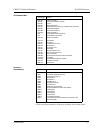
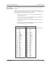
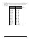
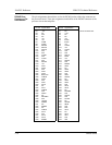
The PCI Local Bus pin assignments shown below are for the PCI option slots on the
backplane.
The PCI Local Bus specifies both 5-volt and 3.3-volt signaling environments. The
following bus pin assignments are for the 5-volt connector. The 3.3-volt connector bus
pin assignments are the same with the following exceptions:
* The pins noted as +V (I/O) are +5 volts or +3.3 volts, depending on which
connector is being used.
† Pins B12, B13, A12 and A13 are Gnd (ground) on the 5-volt connector, but
are Connector Keys on the 3.3-volt connector.
†† Pin B49 is Gnd (ground) on the 5-volt connector, but is M66EN on the 3.3-
volt connector.
††† Pins B50, B51, A50 and A51 are Connectors Keys on the 5-volt connector,
but are Gnd (ground) on the 3.3-volt connector.
I/O Pin Signal Name I/O Pin Signal Name
B1
B2
B3
B4
B5
B6
B7
B8
B9
B10
B11
B12
B13
B14
B15
B16
B17
B18
B19
B20
B21
B22
B23
B24
B25
B26
B27
B28
B29
B30
B31
B32
B33
B34
B35
-12V
TCK
Gnd
TDO
+5V
+5V
INTB#
INTD#
PRSNT1#
Reserved
PRSNT2#
Gnd
†
Gnd †
Reserved
Gnd
CLK
Gnd
REQ#
+V (I/O) *
AD31
AD29
Gnd
AD27
AD25
+3.3V
C/BE3#
AD23
Gnd
AD21
AD19
+3.3V
AD17
C/BE2#
Gnd
IRDY#
A1
A2
A3
A4
A5
A6
A7
A8
A9
A10
A11
A12
A13
A14
A15
A16
A17
A18
A19
A20
A21
A22
A23
A24
A25
A26
A27
A28
A29
A30
A31
A32
A33
A34
A35
TRST#
+12V
TMS
TDI
+5V
INTA#
INTC#
+5V
Reserved
+V (I/O) *
Reserved
Gnd
†
Gnd †
Reserved
RST#
+V (I/O) *
GNT#
Gnd
Reserved
AD30
+3.3V
AD28
AD26
Gnd
AD24
IDSEL
+3.3V
AD22
AD20
Gnd
AD18
AD16
+3.3V
FRAME#
Gnd
32-bit connector start


