


KS152JB Universal Communications Controller
Technical Specifications
Kawasaki LSI USA, Inc. Page 112 of 120 Ver. 0.9 KS152JB2
UR - Underrun Flag, see TSTAT.
XRCLK - External GSC Receive Clock Enable bit, see PCON.
XTCLK - External GSC Transmit Clock Enable bit, see GMOD.
...............................
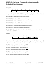
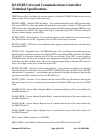
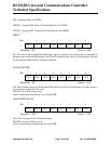
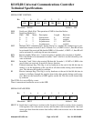
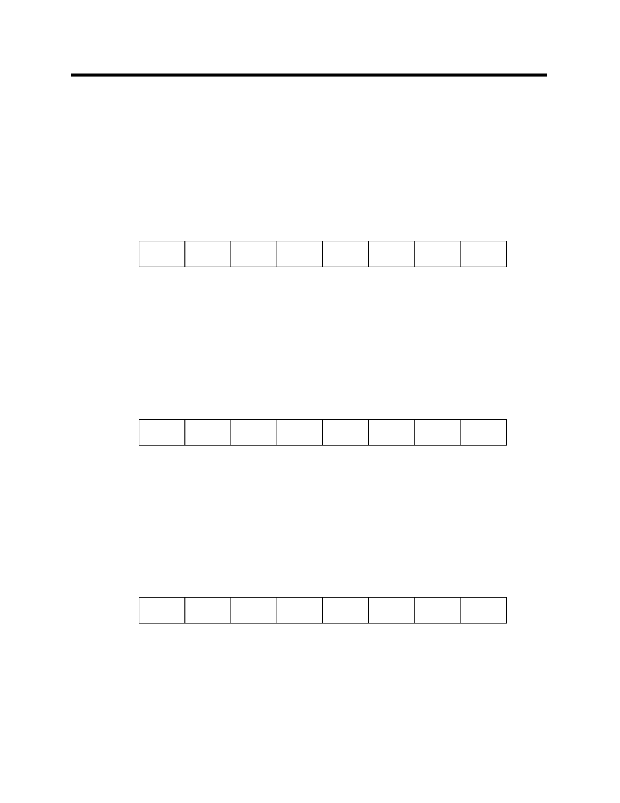
PORT 0
Port 0 is used as the multiplexed address/data bus for external access.Since the cpu executes all
program code from external memory, the Port P0 should not be used for I/O purposes. Pull-ups
are not required when used as a memory interface.
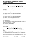
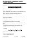
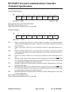
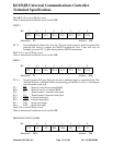
STACK POINTER
The Stack Pointer stores the Scratchpad RAM address where the stack begins. In other words it
always points to the top of the stack.
The SP is set to 07h on any reset.
There is unrestricted read/write access to this SFR.
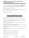
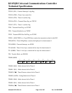
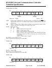
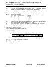
DATA POINTER LOW
This is the low byte of the 16-bit data pointer.
The DPL is reset to 00h by a reset.
There is unrestricted read/write access to this SFR.
P0.6
6
P0.5
5
P0.3
3
P0.7
7
P0.2
2
P0.1
1
P0.0
0
P0.4
4
Bit:
Mnemonic: P0 Address: 80h
SP.6
6
SP.5
5
SP.3
3
SP.7
7
SP.2
2
SP.1
1
SP.0
0
SP.4
4
Bit:
Mnemonic: SP Address: 81h
DPL.6
6
DPL5
5
DPL.3
3
DPL.7
7
DPL.2
2
DPL.1
1
DPL.0
0
DPL.4
4
Bit:
Mnemonic: DPL Address: 82h