


KS152JB Universal Communications Controller
Technical Specifications
Kawasaki LSI USA, Inc. Page 8 of 120 Ver. 0.9 KS152JB2
2.4 PORT STRUCTURES AND OPERATION
The ports are all bidirectional. Each port consists of two sections, the port SFR and the I/O pad.
The Ports 0 and 2 are involved in accesses to external memory. In this case, Port 0 outputs the
lower byte of the external memory address while port 2 outputs the higher byte of the external
address. The Port 0 bus is also used as a data bus for the data byte that is read or is to be written.
Therefore Port 0 is actually a time-multiplexed address/data bus. A point to note is that Port 2 out-
puts the upper 8 bits of the address only if the address is 16 bits wide, else it continues to emit the
Port 2 SFR contents.
In order that the alternate functions on the port pin are activated correctly, the corresponding bit
latch must be held at value 1. If this is not done then the corresponding port pin is stuck at 0, and
external or internal inputs will have no effect on the pin value.
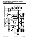
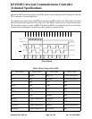
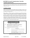
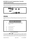
I/O CONFIGURATIONS
Each individual port has different I/O pads to accommodate the different functions of each indi-
vidual port. The figure below shows a simplified diagram of the I/O pads for each port.
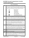
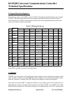
IP XXX00000B SCON 00H
IE 0XX00000B SBUF INDETERMINATE
TMOD 00H PCON 0XXX0000B
TCON 00H DARL0-1 INDETERMINATE
DCON0-1 00H DARh0-1 INDETERMINATE
GMOD X0000000B IFS 00H
IEN1 XX000000B MYSLOT 00H
IPN1 XX000000B PRBS 00H
TCDCNT INDETERMINATE TCON 00H
TFIFO INDETERMINATE TSTAT XX000100B
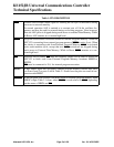
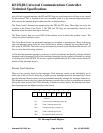
Table 3: Reset Values of the SFRs
SFR Name Reset Value SFR Name Reset Value