KS152JB Universal Communications Controller
Technical Specifications
Kawasaki LSI USA, Inc. Page 80 of 120 Ver. 0.9 KS152JB2
is still 1 and the DONE bit is still 0. An external interrupt is not generated in this case, since in
level-activated mode, pulling the pin to a logical 1 clears the interrupt flag. If the interrupt pin is
then pulled low again, DMA transfers will continue from where they were previously stopped.
The timing for the DMA Cycle in the transition - activated mode, or for the first DMA Cycle in
the level-activated mode is as follows: If the 1-to-0 transition is detected before the final machine
cycle of the instruction in progress, then the DMA commences as soon as the instruction in
progress is completed. Otherwise, one more instruction will be executed before the DMA starts.
No instruction is executed during any DMA Cycle.
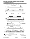
4.2 Timing Diagrams
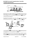
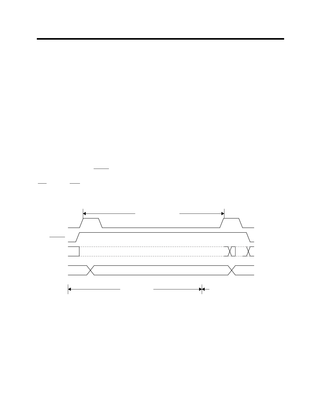
Timing diagrams for single-byte DMA transfers are shown in following figures for four kinds of
DMA Cycles: internal memory to internal memory, internal memory to external memory, external
memory to internal memory, and external memory to external memory. In each case we assume
the C152 is executing out of external program memory. If the C152 is executing out of internal
program memory, the
PSEN is inactive, and the Port 0 and Port 2 pins emit P0 and P2 SFR data. If
External Data Memory is involved, the Port 0 and Port 2 pins are used as the address/data bus, and
RD and /or WR signals are generated as needed, in the same manner as in the execution of a
MOVX @ DPTR instruction.
DMA Transfer from Internal Memory to Internal Memory
12 OSC.PERIODS
ALE
PSEN
P1 INST
P2 PCH
FLOAT
P2 SFR
PCL FLOAT INST
PCH
DMA CYCLE RESUME PROGRAM
EXECUTION


