


KS152JB Universal Communications Controller
Technical Specifications
Kawasaki LSI USA, Inc. Page 116 of 120 Ver. 0.9 KS152JB2
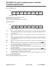
SERIAL PORT CONTROL
SM0 Serial port, Mode 0 bit: The operation of SM0 is described below. .
SM1 Serial port Mode bit 1:
SM0 SM1 Mode Description Length Baud rate
0 0 0 Synchronous 8 4/12 tclk
0 1 1 Asynchronous 10 variable
1 0 2 Asynchronous 11 64/32 tclk
1 1 3 Asynchronous 11 variable
SM2 Multiple MCU communication: Setting this bit to 1 enables the multiprocessor com-
munication feature in mode 2 and 3. In mode 2 or 3, if SM2 is set to 1, then RI will not
be activated if the received 9th data bit (RB8) is 0. In mode 1, if SM2 = 1, then RI will
not be activated if a valid stop bit was not received.
REN Receive enable: When set to 1 serial reception is enabled, else reception is disabled.
TB8 This is the 9th bit to be transmitted in modes 2 and 3. this bit is set and cleared by soft-
ware as desired.
RB8 In modes 2 and 3 this is the received 9th data bit. In mode 1, if SM2 = 0, RB8 is the
stop bit that was received. In mode 0 it has no function.
TI Transmit interrupt flag: This flag is set by hardware at the end of the 8th bit time in
mode 0, or at the beginning of the stop bit in all other modes during serial transmis-
sion. This bit must be cleared by software.
RI Receive interrupt flag: This flag is set by hardware at the end of the 8th bit time in
mode 0, or halfway through the stop bits time in the other modes during serial recep-
tion. However the restrictions of SM2 applies on this bit. This bit can be cleared only
by software
The SCON sfr is set to 00h by a reset.
There is unrestricted read/write access to this SFR.
SERIAL DATA BUFFER
SBUF.7-0 Serial data is read from or written to this location. It actually consists of two separate
8-bit registers. On is the receive resister, and the other is the transmit buffer. Any read
access gets data from the receive data buffer, while write accesses are to the transmit
data buffer.
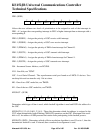
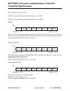
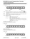
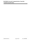
SM1
6
SM2
5
TB8
3
SM0
7
RB8
2
TI
1
RI
0
REN
4
Bit:
Mnemonic: SCON Address: 98h
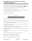
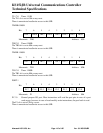
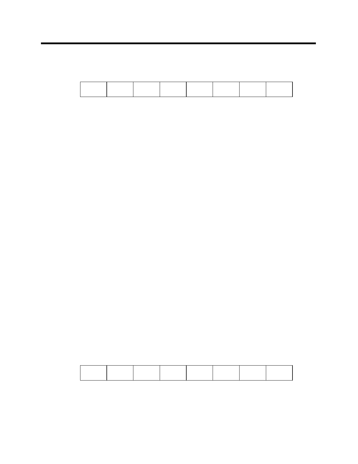
SBUF.6
6
SBUF.5
5
SBUF.3
3
SBUF.7
7
SBUF.2
2
SBUF.1
1
SBUF.0
0
SBUF.4
4
Bit:
Mnemonic: SBUF Address: 99h