


NE-4100 Series User’s Manual Getting Started
3-5
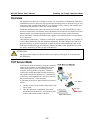
Note that the RS-485 interface is selected on the evaluation board for the NE-4110A and
NE-4120A modules, even when the module is operating in RS-422 mode. Please refer to
Chapter 2
-
Panel Layout and Pin Assignments for additional details.
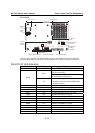
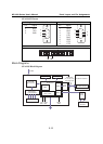
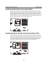
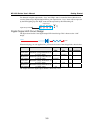
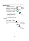
Circuit Pad for External Connection
A circuit pad is provided on the right side of each evaluation board for the development of
additional application circuits.
1234
ON
DIP
910
1314
12
12
5V
3.3V
12
J9
J10
J3
910
12
1314
J4
GND
The first row of the circuit pad is for connecting a 5V power supply; the second row is for
connecting a 3.3V power supply. The last row of the circuit pad is for grounding. Serial signals are
mapped to J3 as an extension of jumper block J9. DIO and LED signals are mapped to J4 as an
extension of jumper block J10. This means that pin assignments for J3 on the circuit pad are the
same as the pin assignments for jumper block J9; pin assignments for J4 on the circuit pad are the
same as the pin assignments for jumper block J10.
5V
3.3V
12
910
12
J9
13 14
12
J10
J3
910
12
13 14
J4
GND
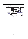
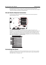
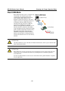
Connecting the Power
Connect the 12 VDC power line with the evaluation board’s power jack. If the power is properly
supplied, the power LED will show a solid red color until the system is ready, at which time the
ready LED will show a solid green color.