


287
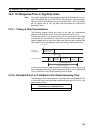
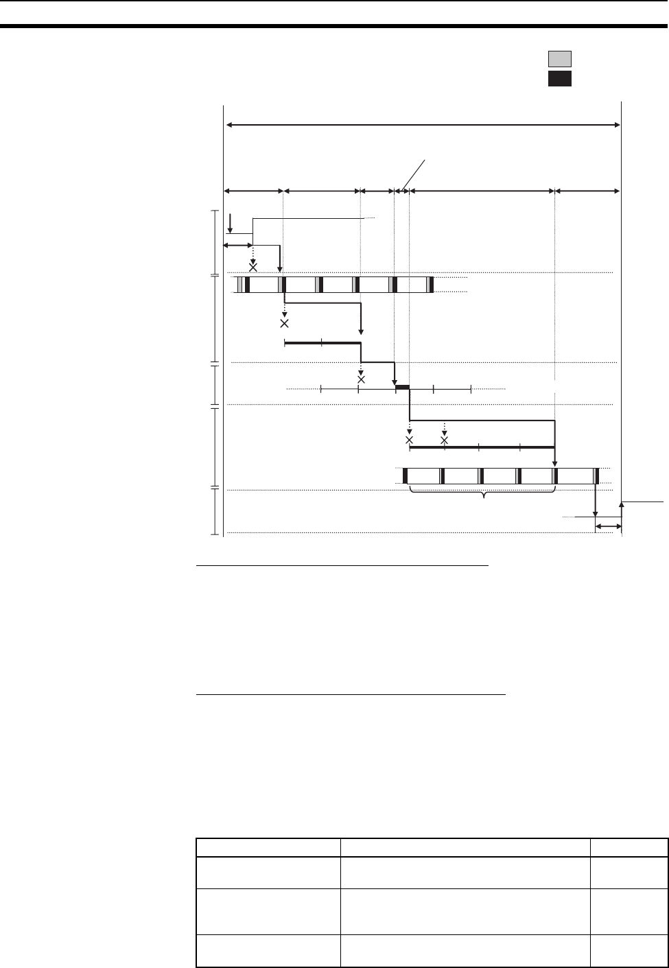
I/O Response Time in Tag Data Links Section 10-3
(1) Node 1 (PLC #1) Input ON Response Time
This is the delay time for the external input device from when the input occurs
until the switch actually turns ON and the time until the input data is stored in
the memory area of the CPU Unit for PLC #1. In this system, the input switch
delay time is 1.5 ms. Also, one CPU cycle time is required until the data is
stored in the memory area of the CPU Unit. Therefore, the input ON response
time is 1.5 ms + 10 ms, or 11.5 ms.
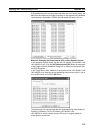
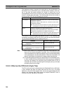
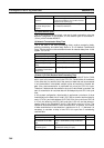
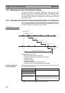
(2) Node 1 (PLC #1) Send Data Processing Time
This is the time until memory data in the CPU Unit is transferred to the Ether-
Net/IP Unit. If the amount of data that can be processed in one data transmis-
sion with the CPU Unit is exceeded, data transmission will be performed over
multiple cycles of the CPU Unit, and so time is calculated for the number of
transmissions times the CPU Unit cycle times. The following table gives the
send data processing times and breakdown for node 1 (PLC #1) in this sys-
tem configuration. Refer to 10-3-2 EtherNet/IP Unit or CJ2H Built-in Port Data
Processing Time for details on the calculation formula for each item.
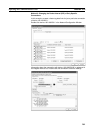
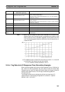
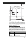
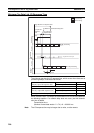
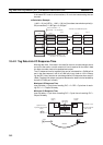
Output
: I/O processing
: Data exchange
Tag data link I/O response time
(1) Input ON
response
time
(2) Send data
processing
time
(3) RPI
(4) Network transmission delay time
(5) Receive data
processing time
(6) Output ON
response time
Input
Calcu-
lation
Calcu-
lation
PLC #1 processing
Send data processing time
Cycle time x 2
Tag data link refresh cycle
Receive data processing time
PLC #2 processing
Input device
Transmission
path
Output
device
PLC #1
PLC #2
Cycle time x 4
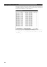
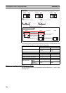
Item Calculation formula Time
A CPU Unit cycle time
for PLC #1
10 m sec
B Number of transmis-
sions based on the data
size
Number of data transmission words (11,552
words) ÷ 6,432 words (using a CJ2 CPU
Unit)
2
C EtherNet/IP Unit data
processing time
0.0008 × 6,432 + 1.0 (Maximum number of
transmission words per cycle)
6.15 m sec