Appendix A Connector Signal Descriptions 215
Reference for the Universal Serial Bus
(USB) Connectors
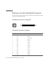
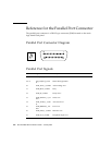
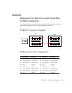
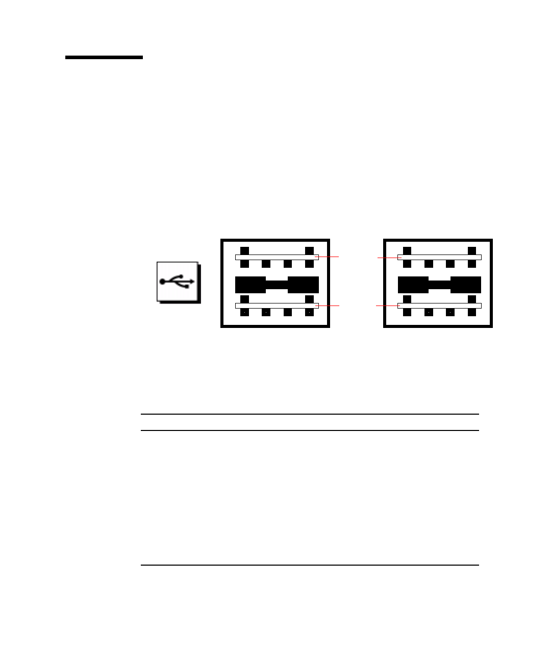
Four Universal Serial Bus (USB) connectors (J3001, J3002) are located on the main
logic board back panel. The port pin assignments are identical.
USB Port Connector Diagram
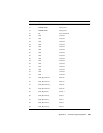
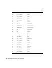
USB Connector Pin Assignments
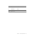
Pin Signal Name Description Pin Signal Name Description
A1 USB0_VCC 5 Volts C1 USB2_VCC 5 Volts
A2 CM_USB_D0_N Signal negative C2 CM_USB_D0_N Signal negative
A3 CM_USB_D0_P Signal positive C3 CM_USB_D0_P Signal positive
A4 Gnd Ground C4 Gnd Ground
B1 USB1_VCC 5 Volts D1 USB3_VCC 5 Volts
B2 CM_USB_D1_N Signal negative D2 CM_USB_D1_N Signal negative
B3 CM_USB_D1_P Signal positive D3 CM_USB_D1_P Signal positive
B4 Gnd Ground D4 Gnd Ground
1234
1234
A
B
1234
1234
J3001
J3002
C
D


