


Intel® Xeon® Processor E5-1600/E5-2600/E5-4600 Product Families 143
Datasheet Volume One
Signal Descriptions
6 Signal Descriptions
This chapter describes the processor signals. They are arranged in functional groups
according to their associated interface or category.
6.1 System Memory Interface Signals
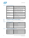
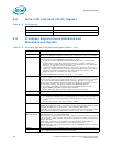
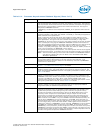
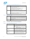
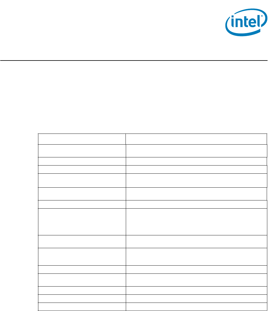
Table 6-1. Memory Channel DDR0, DDR1, DDR2, DDR3
Signal Name Description
DDR{0/1/2/3}_BA[2:0] Bank Address. Defines the bank which is the destination for the
current Activate, Read, Write, or Precharge command.
DDR{0/1/2/3}_CAS_N Column Address Strobe.
DDR{0/1/2/3}_CKE[5:0] Clock Enable.
DDR{0/1/2/3}_CLK_DN[3:0]
DDR{0/1/2/3}_CLK_DP[3:0]
Differential clocks to the DIMM. All command and control signals
are valid on the rising edge of clock.
DDR{0/1/2/3}_CS_N[9:0] Chip Select. Each signal selects one rank as the target of the
command and address.
DDR{0/1/2/3}_DQ[63:00] Data Bus. DDR3 Data bits.
DDR{0/1/2/3}_DQS_DP[17:00]
DDR{0/1/2/3}_DQS_DN[17:00]
Data strobes. Differential pair, Data/ECC Strobe. Differential
strobes latch data/ECC for each DRAM. Different numbers of
strobes are used depending on whether the connected DRAMs are
x4,x8. Driven with edges in center of data, receive edges are
aligned with data edges.
DDR{0/1/2/3}_ECC[7:0] Check bits. An error correction code is driven along with data on
these lines for DIMMs that support that capability
DDR{0/1/2/3}_MA[15:00] Memory Address. Selects the Row address for Reads and writes,
and the column address for activates. Also used to set values for
DRAM configuration registers.
DDR{0/1/2/3}_MA_PAR Odd parity across Address and Command.
DDR{0/1/2/3}_ODT[5:0] On Die Termination. Enables DRAM on die termination during Data
Write or Data Read transactions.
DDR{0/1/2/3}_PAR_ERR_N Parity Error detected by Registered DIMM (one for each channel).
DDR{0/1/2/3}_RAS_N Row Address Strobe.
DDR{0/1/2/3}_WE_N Write Enable.