


Intel® Xeon® Processor E5-1600/E5-2600/E5-4600 Product Families 177
Datasheet Volume One
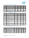
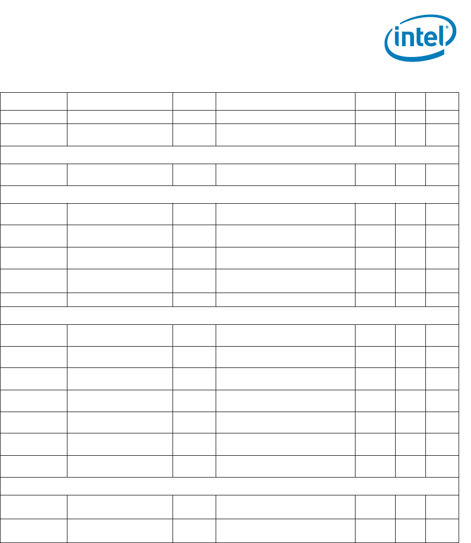
Notes:
1. Unless otherwise noted, all specifications in this table apply to all processor frequencies.
2. The voltage rail V
CCD
which will be set to 1.50 V or 1.35 V nominal depending on the voltage of all DIMMs connected to the
processor.
3. V
IL
is the maximum voltage level at a receiving agent that will be interpreted as a logical low value.
4. V
IH
is the minimum voltage level at a receiving agent that will be interpreted as a logical high value.
5. V
IH
and V
OH
may experience excursions above V
CCD
. However, input signal drivers must comply with the signal quality
specifications. Refer to Section 7.9.
6. This is the pull down driver resistance. Refer to processor signal integrity models for I/V characteristics. Reset drive does not
have a termination.
7. R
VTT_TERM
is the termination on the DIMM and not controlled by the processor. Please refer to the applicable DIMM datasheet.
8. The minimum and maximum values for these signals are programmable by BIOS to one of the pairs.
9. COMP resistance must be provided on the system board with 1% resistors. See the
applicable platform design guide for
implementation details. DDR01_RCOMP[2:0] and DDR23_RCOMP[2:0] resistors are terminated to VSS.
10. Input leakage current is specified for all DDR3 signals.
11. DRAM_PWR_OK_C{01/23} must have a maximum of 30 ns rise or fall time over VCCD * 0.55 +300 mV and -200 mV and the
edge must be monotonic.
12. The DDR01/23_RCOMP error tolerance is ± 15% from the compensated value.
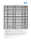
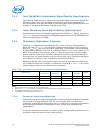
V
OL
Output Low Voltage (V
CCD
/ 2)* (R
ON
/(R
ON
+R
VTT_TERM
)) V 2, 7
V
OH
Output High Voltage V
CCD
- ((V
CCD
/ 2)* (R
ON
/
(R
ON
+R
VTT_TERM
))
V2, 5, 7
Reference Clock Signal
R
ON
DDR3 Clock Buffer On
Resistance
21 31 Ω 6
Command Signals
R
ON
DDR3 Command Buffer On
Resistance
16 24 Ω 6
R
ON
DDR3 Reset Buffer On
Resistance
25 75 Ω 6
V
OL_CMOS1.5v
Output Low Voltage, Signals
DDR_RESET_ C{01/23}_N
0.2*V
CCD
V1,2
V
OH_CMOS1.5v
Output High Voltage, Signals
DDR_RESET_ C{01/23}_N
0.9*V
CCD
V1,2
I
IL_CMOS1.5v
Input Leakage Current -100 +100 μA1,2
Control Signals
R
ON
DDR3 Control Buffer On
Resistance
21 31 Ω 6
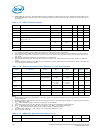
DDR01_RCOMP[0
]
COMP Resistance 128.7 130 131.3
Ω 9,12
DDR01_RCOMP[1
]
COMP Resistance 25.839 26.1 26.361
Ω 9,12
DDR01_RCOMP[2
]
COMP Resistance 198 200 202
Ω 9,12
DDR23_RCOMP[0
]
COMP Resistance 128.7 130 131.3
Ω 9,12
DDR23_RCOMP[1
]
COMP Resistance 25.839 26.1 26.361
Ω 9,12
DDR23_RCOMP[2
]
COMP Resistance 198 200 202
Ω 9,12
DDR3 Miscellaneous Signals
V
IL
Input Low Voltage
DRAM_PWR_OK_C{01/23}
0.55*VCC
D - 0.2
V2, 3,
11, 13
V
IH
Input High Voltage
DRAM_PWR_OK_C{01/23}
0.55*VCC
D + 0.3
V 2, 4, 5,
11, 13
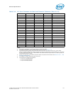
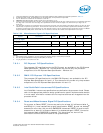
Table 7-16. DDR3 and DDR3L Signal DC Specifications (Sheet 2 of 2)
Symbol Parameter Min Typ Max Units Notes
1