Electrical Specifications
160 Intel® Xeon® Processor E5-1600/E5-2600/E5-4600 Product Families
Datasheet Volume One
Notes:
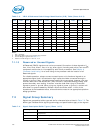
1. 00h = Off State
2. VID Range HEX 01-32 are not used by the processor.
3. For VID Ranges supported see Table 7-11.
4. VCCD is a fixed voltage of 1.35 V or 1.5 V.
7.1.10 Reserved or Unused Signals
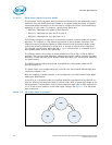
All Reserved (RSVD) signals must not be connected. Connection of these signals to V
CC
,
V
TTA
, V
TTD
, V
CCD,
V
CCPLL
, V
SS
, or to any other signal (including each other) can result in
component malfunction or incompatibility with future processors. See Chapter 8,
“Processor Land Listing” for a land listing of the processor and the location of all
Reserved signals.
For reliable operation, always connect unused inputs or bi-directional signals to an
appropriate signal level. Unused active high inputs should be connected through a
resistor to ground (V
SS
). Unused outputs maybe left unconnected; however, this may
interfere with some Test Access Port (TAP) functions, complicate debug probing, and
prevent boundary scan testing. A resistor must be used when tying bi-directional
signals to power or ground. When tying any signal to power or ground, a resistor will
also allow for system testability. Resistor values should be within ± 20% of the
impedance of the baseboard trace, unless otherwise noted in the appropriate platform
design guidelines.
7.2 Signal Group Summary
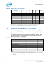
Signals are grouped by buffer type and similar characteristics as listed in Table 7-5. The
buffer type indicates which signaling technology and specifications apply to the signals.
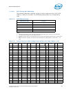
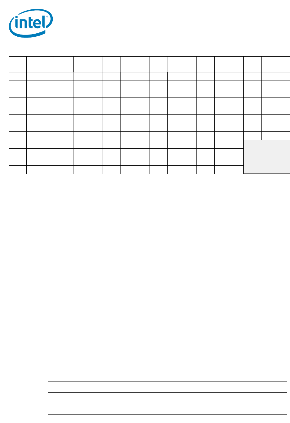
49 0.61000 6C 0.78500 8F 0.96000 B2 1.13500 D5 1.31000 F8 1.48500
4A 0.61500 6D 0.79000 90 0.96500 B3 1.14000 D6 1.31500 F9 1.49000
4B 0.62000 6E 0.79500 91 0.97000 B4 1.14500 D7 1.32000 FA 1.49500
4C 0.62500 6F 0.80000 92 0.97500 B5 1.15000 D8 1.32500 FB 1.50000
4D 0.63000 70 0.80500 93 0.98000 B6 1.15500 D9 1.33000 FC 1.50500
4E 0.63500 71 0.81000 94 0.98500 B7 1.16000 DA 1.33500 FD 1.51000
4F 0.64000 72 0.81500 95 0.99000 B8 1.16500 DB 1.34000 FE 1.51500
50 0.64500 73 0.82000 96 0.99500 B9 1.17000 DC 1.34500 FF 1.52000
51 0.65000 74 0.82500 97 1.00000 BA 1.17500 DD 1.35000
52 0.65500 75 0.83000 98 1.00500 BB 1.18000 DE 1.35500
53 0.66000 76 0.83500 99 1.01000 BC 1.18500 DF 1.36000
54 0.66500 77 0.84000 9A 1.01500 BD 1.19000 E0 1.36500
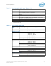
Table 7-3. VR12.0 Reference Code Voltage Identification (VID) Table (Sheet 2 of 2)
HEX
VCC, VSA,
VCCD
HEX
VCC, VSA,
VCCD
HEX
VCC, VSA,
VCCD
HEX
VCC, VSA,
VCCD
HEX
VCC, VSA,
VCCD
HEX
VCC, VSA,
VCCD
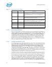
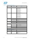
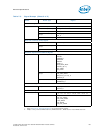
Table 7-4. Signal Description Buffer Types (Sheet 1 of 2)
Signal Description
Analog Analog reference or output. May be used as a threshold voltage or for buffer
compensation
Asynchronous
1
Signal has no timing relationship with any system reference clock.
CMOS CMOS buffers: 1.05 V or 1.5 V tolerant


