


Intel® Xeon® Processor E5-1600/E5-2600/E5-4600 Product Families 169
Datasheet Volume One
Electrical Specifications
7.8.1 Voltage and Current Specifications
Notes:
1. Unless otherwise noted, all specifications in this table apply to all processors. These specifications are based on final silicon
characterization.
2. Individual processor VID values may be calibrated during manufacturing such that two devices at the same speed may have
different settings.
3. These voltages are targets only. A variable voltage source should exist on systems in the event that a different voltage is
required.
4. The V
CC
voltage specification requirements are measured across the remote sense pin pairs (VCC_SENSE and
VSS_VCC_SENSE) on the processor package. Voltage measurement should be taken with a DC to 100 MHz bandwidth
oscilloscope limit (or DC to 20 MHz for older model oscilloscopes), using a 1.5 pF maximum probe capacitance, and 1M
Ω
minimum impedance. The maximum length of the ground wire on the probe should be less than 5 mm to ensure external
noise from the system is not coupled in the scope probe.
5. The V
TTA,
and V
TTD
voltage specification requirements are measured across the remote sense pin pairs (VTTD_SENSE and
VSS_VTTD_SENSE) on the processor package. Voltage measurement should be taken with a DC to 100 MHz bandwidth
oscilloscope limit (or DC to 20 MHz for older model oscilloscopes), using a 1.5 pF maximum probe capacitance, and 1M
Ω
minimum impedance. The maximum length of the ground wire on the probe should be less than 5 mm to ensure external
noise from the system is not coupled in the scope probe.
6. The V
SA
voltage specification requirements are measured across the remote sense pin pairs (VSA_SENSE and
VSS_VSA_SENSE) on the processor package. Voltage measurement should be taken with a DC to 100 MHz bandwidth
oscilloscope limit (or DC to 20 MHz for older model oscilloscopes), using a 1.5 pF maximum probe capacitance, and 1M
Ω
minimum impedance. The maximum length of the ground wire on the probe should be less than 5 mm to ensure external
noise from the system is not coupled in the scope probe.
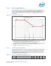
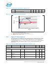
7. For the 8/6-core processor refer to Table 7-13 and corresponding Figure 7-3. For the 4/2-core processor refer to Table 7-14
and corresponding Figure 7-4.The processor should not be subjected to any static V
CC
level that exceeds the V
CC_MAX
associated with any particular current. Failure to adhere to this specification can shorten processor lifetime.
8. Minimum V
CC
and maximum I
CC
are specified at the maximum processor case temperature (T
CASE
) shown in Section 5,
“Thermal Management Specifications”. I
CC_MAX
is specified at the relative V
CC_MAX
point on the V
CC
load line. The processor is
capable of drawing I
CC_MAX
for up to 5 seconds. Refer to Figure 7-5 for further details on the average processor current draw
over various time durations.
9. The processor should not be subjected to any static V
TTA,
V
TTD
level that exceeds the V
TT_MAX
associated with any particular
current. Failure to adhere to this specification can shorten processor lifetime.
10. This specification represents the V
CC
reduction or V
CC
increase due to each VID transition, see Section 7.1.9.3, “Voltage
Identification (VID)”.
11. Baseboard bandwidth is limited to 20 MHz.
12. FMB is the flexible motherboard guidelines. See Section 7.6 for FMB details.
13. DC + AC + Ripple = Total Tolerance
14. For Power State Functions see Section 7.1.9.3.5.
15. V
SA_VID
does not have a loadline, the output voltage is expected to be the VID value.
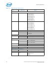
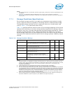
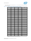
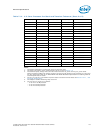
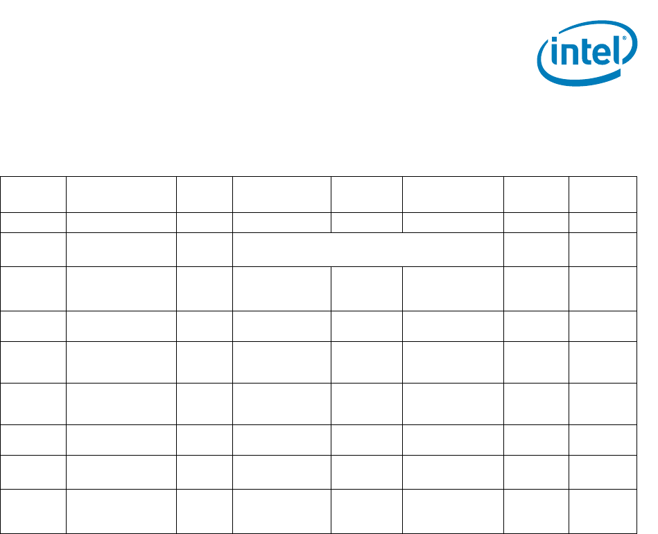
Table 7-11. Voltage Specification
Symbol Parameter
Voltage
Plane
Min Typ Max Unit Notes
1
V
CC
VID V
CC
VID Range 0.6 1.35 V 2, 3
V
CC
Core Voltage
(Launch - FMB)
V
CC
See Table 7-13, Table 7-14 and Figure 7-3, Figure 7-4 V 3, 4, 7, 8,
12, 14, 18
V
VID_STEP
(Vcc, Vsa,
Vccd)
VID step size during
a transition
5.0 mV 10
V
CCPLL
PLL Voltage V
CCPLL
0.955*V
CCPLL_TYP
1.8 1.045*V
CCPLL_TYP
V 11, 12, 13,
17
V
CCD
(V
CCD_01,
V
CCD_23)
I/O Voltage for DDR3
(Standard Voltage)
V
CCD
0.95*V
CCD_TYP
1.5 1.05*V
CCD_TYP
V 11, 13, 14,
16, 17
V
CCD
(V
CCD_01.
V
CCD_23)
I/O Voltage for
DDR3L (Low Voltage)
V
CCD
0.95*V
CCD_TYP
1.35 1.075*V
CCD_TYP
V 11, 13, 14,
16, 17
V
TT
(V
TTA,
VTTD)
Uncore Voltage
(Launch - FMB)
V
TT
0.957*V
TT_TYP
1.05 1.043*V
TT_TYP
V 3, 5, 9, 12,
13
V
SA_VID
Vsa VID Range V
SA
0.6 0.965 1.20 V 2, 3, 14, 15
V
SA
System Agent
Voltage
(Launch - FMB)
V
SA
V
SA_VID
- 0.064 V
SA_VID
V
SA_VID
+ 0.064 V 3, 6, 12, 14,
19