


Signal Descriptions
144 Intel® Xeon® Processor E5-1600/E5-2600/E5-4600 Product Families
Datasheet Volume One
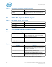
6.2 PCI Express* Based Interface Signals
Note: PCI Express* Ports 1, 2 and 3 Signals are receive and transmit differential pairs.
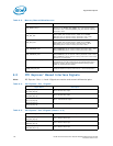
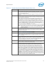
Table 6-2. Memory Channel Miscellaneous
Signal Name Description
DDR_RESET_C01_N
DDR_RESET_C23_N
System memory reset: Reset signal from processor to DRAM
devices on the DIMMs. DDR_RESET_C01_N is used for memory
channels 0 and 1 while DDR_RESET_C23_N is used for memory
channels 2 and 3.
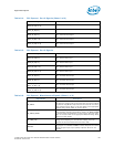
DDR_SCL_C01
DDR_SCL_C23
SMBus clock for the dedicated interface to the serial presence
detect (SPD) and thermal sensors (TSoD) on the DIMMs.
DDR_SCL_C01 is used for memory channels 0 and 1 while
DDR_SCL_C23 is used for memory channels 2 and 3.
DDR_SDA_C01
DDR_SDA_C23
SMBus data for the dedicated interface to the serial presence
detect (SPD) and thermal sensors (TSoD) on the DIMMs.
DDR_SDA_C1 is used for memory channels 0 and 1 while
DDR_SDA_C23 is used for memory channels 2 and 3.
DDR_VREFDQRX_C01
DDR_VREFDQRX_C23
Voltage reference for system memory reads.
DDR_VREFDQRX_C01 is used for memory channels 0 and 1 while
DDR_VREFDQRX_C23 is used for memory channels 2 and 3.
DDR_VREFDQTX_C01
DDR_VREFDQTX_C23
Voltage reference for system memory writes.
DDR_VREFDQTX_C01 is used for memory channels 0 and 1 while
DDR_VREFDQTX_C23 is used for memory channels 2 and 3. These
signals are not connected.
DDR{01/23}_RCOMP[2:0] System memory impedance compensation. Impedance
compensation must be terminated on the system board using a
precision resistor. See the appropriate Platform Design Guide
(PDG) for implementation details.
DRAM_PWR_OK_C01
DRAM_PWR_OK_C23
Power good input signal used to indicate that the VCCD power
supply is stable for memory channels 0 & 1 and channels 2 & 3.
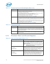
Table 6-3. PCI Express* Port 1 Signals
Signal Name Description
PE1A_RX_DN[3:0]
PE1A_RX_DP[3:0]
PCIe* Receive Data Input
PE1B_RX_DN[7:4]
PE1B_RX_DP[7:4]
PCIe* Receive Data Input
PE1A_TX_DN[3:0]
PE1A_TX_DP[3:0]
PCIe* Transmit Data Output
PE1B_TX_DN[7:4]
PE1B_TX_DP[7:4]
PCIe* Transmit Data Output
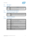
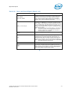
Table 6-4. PCI Express* Port 2 Signals (Sheet 1 of 2)
Signal Name Description
PE2A_RX_DN[3:0]
PE2A_RX_DP[3:0]
PCIe* Receive Data Input
PE2B_RX_DN[7:4]
PE2B_RX_DP[7:4]
PCIe* Receive Data Input
PE2C_RX_DN[11:8]
PE2C_RX_DP[11:8]
PCIe* Receive Data Input