


178 Intel® Xeon® Processor E5-1600/E5-2600/E5-4600 Product Families
Datasheet Volume One
13. DRAM_PWR_OK_C{01/23}: Data Scrambling must be enabled for production environments. Disabling Data scrambling may
be used for debug and testing purposes only. Operating systems with Data Scrambling off will make the configuration out of
specification.
Notes:
1. V
TTD
supplies the PECI interface. PECI behavior does not affect V
TTD
min/max specification
2. It is expected that the PECI driver will take into account, the variance in the receiver input thresholds and consequently, be
able to drive its output within safe limits (-0.150 V to 0.275*V
TTD
for the low level and 0.725*V
TTD
to V
TTD
+0.150 V for the
high level).
3. The leakage specification applies to powered devices on the PECI bus.
4. One node is counted for each client and one node for the system host. Extended trace lengths might appear as additional
nodes.
5. Excessive capacitive loading on the PECI line may slow down the signal rise/fall times and consequently limit the maximum bit
rate at which the interface can operate.
Notes:
1. Unless otherwise noted, all specifications in this table apply to all processor frequencies. These specifications are specified at
the processor pad.
2. Crossing Voltage is defined as the instantaneous voltage value when the rising edge of BCLK{0/1}_DN is equal to the falling
edge of BCLK{0/1}_DP.
3. V
Havg
is the statistical average of the VH measured by the oscilloscope.
4. The crossing point must meet the absolute and relative crossing point specifications simultaneously.
5. V
Havg
can be measured directly using “Vtop” on Agilent* and “High” on Tektronix oscilloscopes.
6. V
CROSS
is defined as the total variation of all crossing voltages as defined in Note 3.
7. The rising edge of BCLK{0/1}_DN is equal to the falling edge of BCLK{0/1}_DP.
8. For Vin between 0 and Vih.
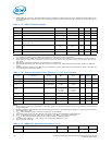
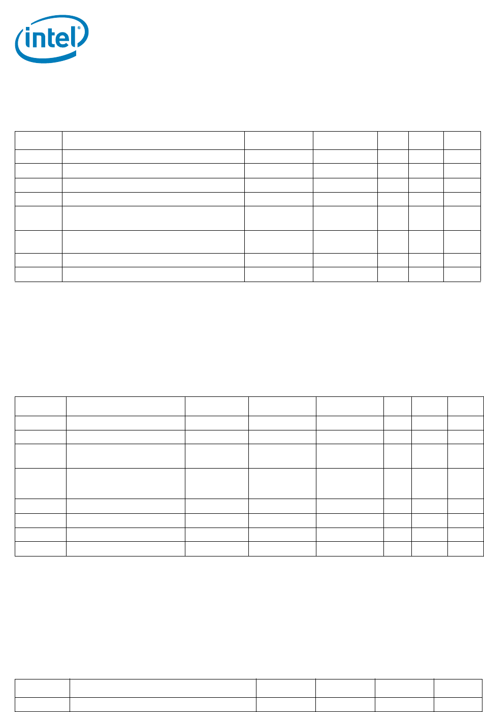
Table 7-17. PECI DC Specifications
Symbol Definition and Conditions Min Max Units Figure Notes
1
V
In
Input Voltage Range -0.150 V
TT
V
V
Hysteresis
Hysteresis 0.100 * V
TT
V
V
N
Negative-edge threshold voltage 0.275 * V
TT
0.500 * V
TT
V 7-1 2
V
P
Positive-edge threshold voltage 0.550 * V
TT
0.725 * V
TT
V 7-1 2
I
SOURCE
High level output source
V
OH
= 0.75 * V
TT
-6.0 mA
I
Leak+
High impedance state leakage to V
TTD
(V
leak
=
V
OL
)
50 200 µA 3
C
Bus
Bus capacitance per node N/A 10 pF 4,5
V
Noise
Signal noise immunity above 300 MHz 0.100 * V
TT
N/A V
p-p
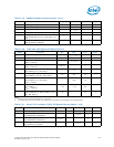
Table 7-18. System Reference Clock (BCLK{0/1}) DC Specifications
Symbol Parameter Signal Min Max
Unit Figure Notes
1
V
BCLK_diff_ih
Differential Input High Voltage Differential 0.150 N/A V 7-8
V
BCLK_diff_il
Differential Input Low Voltage Differential -0.150 V 7-8
V
cross
(abs) Absolute Crossing Point
Single Ended 0.250 0.550 V
7-7
7-9
2, 4, 7
V
cross
(rel) Relative Crossing Point Single Ended 0.250 +
0.5*(VH
avg
-
0.700)
0.550 +
0.5*(VH
avg
-
0.700)
V 7-7 3, 4, 5
ΔV
cross
Range of Crossing Points Single Ended N/A 0.140 V 7-10 6
V
TH
Threshold Voltage Single Ended Vcross - 0.1 Vcross + 0.1 V
I
IL
Input Leakage Current N/A 1.50 μA8
C
pad
Pad Capacitance N/A 0.9 1.1 pF
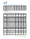
Table 7-19. SMBus DC Specifications (Sheet 1 of 2)
Symbol Parameter Min Max Units Notes
V
IL
Input Low Voltage 0.3*V
TT
V