


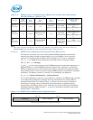
44 Intel® Xeon® Processor E5-1600/E5-2600/E5-4600 Product Families
Datasheet Volume One
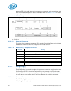
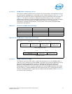
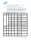
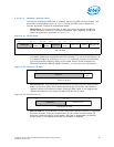
The minimum DRAM power in Figure 2-18 corresponds to a minimum bandwidth
setting of the memory interface. It does ‘not’ correspond to a processor IDLE or
memory self-refresh state. The ‘time window’ in Figure 2-18 is representative of the
rate at which the power control unit (PCU) samples the DRAM energy consumption
information and reactively takes the necessary measures to meet the imposed power
limits. Programming too small a time window may not give the PCU enough time to
sample energy information and enforce the limit while too large a time window runs the
risk of the PCU not being able to monitor and take timely action on energy excursions.
While the DRAM power setting in Figure 2-18 provides a maximum value for the ‘time
window’ (typically a few seconds), the minimum value may be assumed to be
~100 mS.
The PCU programs the DRAM power settings described in Figure 2-18 when DRAM
characterization has been completed by the memory reference code (MRC) during boot
as indicated by the setting of the RST_CPL bit of the BIOS_RESET_CPL register. The
DRAM power settings will be programmed during boot independent of the ‘DRAM Power
Limit Enable’ bit setting. Please refer to the Intel® Xeon® Processor E5 Product Family
Datasheet Volume Two for information on memory energy estimation methods and
energy tuning options used by BIOS and other utilities for determining the range
specified in the DRAM power settings. In general, any tuning of the power settings is
done by polling the voltage regulators supplying the DIMMs.
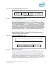
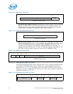
2.5.2.6.9 DRAM Power Limit Data Write / Read
This feature allows the PECI host to program the power limit over a specified time or
control window for the entire DRAM domain covering all the DIMMs within all the
memory channels. Actual values are chosen based on DRAM power consumption
characteristics. The units for the DRAM Power Limit and Control Time Window are
determined as per the Package Power SKU Unit settings described in
Section 2.5.2.6.11. The DRAM Power Limit Enable bit in Figure 2-19 should be set to
activate this feature. Exact DRAM power limit values are largely determined by platform
memory configuration. As such, this feature is disabled by default and there are no
defaults associated with the DRAM power limit values. The PECI host may be used to
enable and initialize the power limit fields for the purposes of DRAM power budgeting.
Alternatively, this can also be accomplished through inband writes to the appropriate
registers. Both power limit enabling and initialization of power limit values can be done
in the same command cycle. All RAPL parameter values including the power limit value,
control time window, and enable bit will have to be specified correctly even if the intent
is to change just one parameter value when programming over PECI.
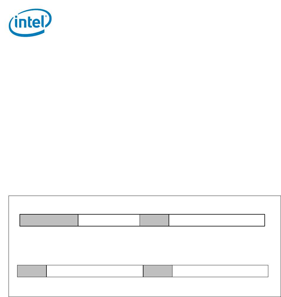
Figure 2-18. DRAM Power Info Read Data
DRAM_POWER_INFO (lower bits)
Reserved
14
Minimum DRAM Power
16
TDP DRAM Power
(Typical Value)
30 015
Reserved
31
DRAM_POWER_INFO (upper bits)
Maximum DRAM Power
3246
Reserved
47
Maximum Time
Window
4854
Reserved
5563