


Intel® Server Board SE7320SP2 & Intel Server Board SE7525GP2 TPS Functional Architecture
Revision 2.0
62
3.7.1.2.3 High BIOS
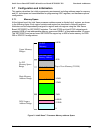
The top 1 MB of Extended Memory under 4GB is reserved for the system BIOS, extended BIOS
for PCI devices, and A20 aliasing by the system BIOS. The lntel Xeon processor begins
executing from the high BIOS region after reset.
3.7.1.2.4 I/O APIC Configuration Space
A 64 KB block located 20 MB below 4 GB (0FEC00000 to 0FEC0FFFFh) is reserved for the I/O
APIC configuration space. The first I/O APIC is located at FEC00000h. The second I/O APIC is
located at FEC80000h. The third I/O APIC is located at FEC80100h.
3.7.1.2.5 Extended lntel
®
Xeon™ Processor Region (above 4GB)
An lntel Xeon processor based system can have up to 64 GB of addressable memory. With the
chipset only supporting 16GB of addressable memory, the BIOS uses an extended addressing
mechanism to use the address ranges.
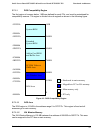
3.7.1.3 Memory Shadowing
System BIOS and option ROM can be shadowed in main memory. Typically this is done to allow
ROM code to execute more rapidly out of RAM. ROM is designated read-only during the copy
process while RAM at the same address is designated write-only. After copying, the RAM is
designated read-only. After the BIOS is shadowed, the attributes for that memory area are set to
read only so that all writes are forwarded to the expansion bus.
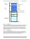
3.7.1.4 System Management Mode Handling
The chipset supports System Management Mode (SMM) operation in one of three modes.
System Management RAM (SMRAM) provides code and data storage space for the SMI_L
handler code, and is made visible to the processor only on entry to SMM, or other conditions
which can be configured using Intel Lindenhurst PF chipset.
The MCH supports three SMM options:
• Compatible SMRAM (C_SMRAM)
• High Segment (HSEG)
• Top of Memory Segment (TSEG)
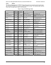
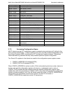
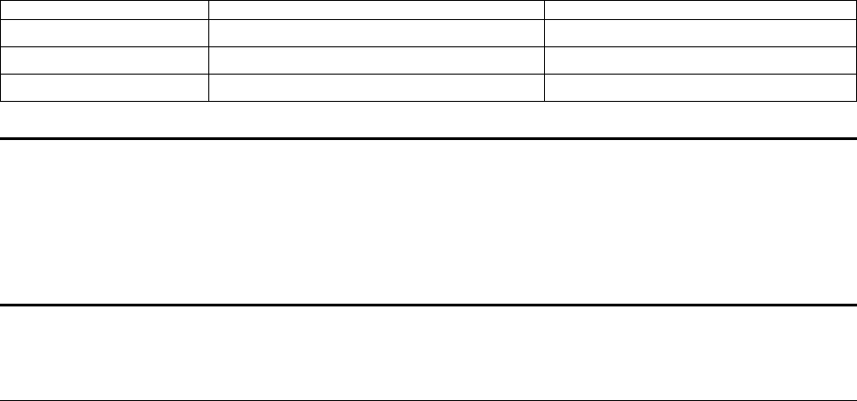
Three abbreviations are used later in the table that describes SMM Space Transaction Handling.
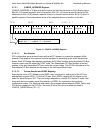
SMM Space Enabled Transaction Address Space (Adr) DRAM Space (DRAM)
Compatible (C) A0000h to BFFFFh A0000h to BFFFFh
High (H) 0FEDA0000h TO 0FEDBFFFFh A0000h to BFFFFh
TSEG (T) (TOLM-TSEG_SZ) to TOLM (TOLM-TSEG_SZ) to TOLM
Notes: High SMM is different than in previous chipsets. In previous chipsets the High segment
was the 384KB region from A_0000h to F_FFFFh. However C_0000h to F_FFFFh was not
useful so it is deleted in MCH.
TSEG SMM is different than in previus chipset. In previous chipsets the TSEG address space
was offset by 256MB to allow for simpler decoding and the TSEG was remapped to directly
under th TOLM. In the MCH the TSEG region is not offset by 256MB and it is not remapped.