


Contents
© National Instruments Corporation vii PC-DIO-96 User Manual
Figures
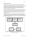
Figure 1-1. The Relationship between the Programming Environment, NI-DAQ, and Your
Hardware ........................................................................................................... 1-3
Figure 2-1. PC -DIO-96 Parts Locator Diagram ................................................................... 2-2
Figure 2-2. Example Base I/O Address Switch Settings...................................................... 2-3
Figure 2-3. Interrupt Jumper Setting for IRQ5 (Factory Setting) ........................................ 2-5
Figure 2-4. Digital I/O Connector Pin Assignments ............................................................ 2-7
Figure 2-5. Cable-Assembly Connector Pinout for Pins 1 through 50 ................................ 2-10
Figure 2-6. Cable-Assembly Connector Pinout for Pins 51 through 100 ............................ 2-11
Figure 2-7. Digital I/O Connections..................................................................................... 2-13
Figure 3-1. PC-DIO-96 Block Diagram ............................................................................... 3-1
Figure 4-1. Control Word Formats for the 82C55A ............................................................ 4-3
Figure 4-2. Control-Word Format for the 8253 ................................................................... 4-4
Tables
Table 2-1. PC-DIO-96 Factory-Set Switch and Jumper Settings ....................................... 2-1
Table 2-2. Switch Settings with Corresponding Base I/O Address
and Base I/O Address Space ............................................................................. 2-4
Table 2-3. Port C Signal Assignments ................................................................................ 2-9
Table 4-1. PC-DIO-96 Address Map .................................................................................. 4-2
Table 4-2. Port C Set/Reset Control Words ........................................................................ 4-4
Table 4-3. Mode 0 I/O Configurations ............................................................................... 4-11
Table A-1. Maximum Average Transfer Rates for the PC-DIO-96 .................................... A-3