


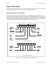

Chapter 4 Register-Level Programming
© National Instruments Corporation 4-11 PC-DIO-96 User Manual
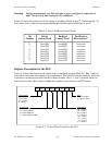
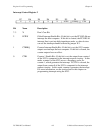
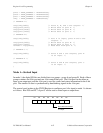
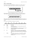
Table 4-3. Mode 0 I/O Configurations
Control Word Group A Group B
Number Bit Port A Port C
1
Port B Port C
2
76543210
0 10000000 Output Output Output Output
1 10000001 Output Output Output Input
2 10000010 Output Output Input Output
3 10000011 Output Output Input Input
4 10001000 Output Input Output Output
5 10001001 Output Input Output Input
6 10001010 Output Input Input Output
7 10001011 Output Input Input Input
8 10010000 Input Output Output Output
9 10010001 Input Output Output Input
10 10010010 Input Output Input Output
11 10010011 Input Output Input Input
12 10011000 Input Input Output Output
13 10011001 Input Input Output Input
14 10011010 Input Input Input Output
15 10011011 Input Input Input Input
1
Upper nibble of port C
2
Lower nibble of port C
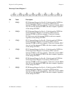
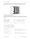
Mode 0 Programming Example
The following example shows how to configure PPI A for various combinations of mode 0 input
and output. This code is strictly an example and is not intended to be used without modification
in a practical situation.
Main() {
#define BASE_ADDRESS 0x180 /* Board located at address 180 */
#define APORTAoffset 0x00 /* Offset for PPI A, port A */
#define APORTBoffset 0x01 /* Offset for PPI A, port B */
#define APORTCoffset 0x02 /* Offset for PPI A, port C */
#define ACNFGoffset 0x03 /* Offset for PPI A, CNFG */
unsigned int porta, portb, portc, cnfg;
char valread; /* Variable to store data read from a
port */
/* Calculate register addresses */