


MOTOROLA MSC8101ADS RevB User’s Manual 37
Operating Instructions
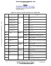
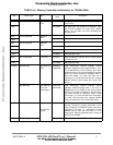
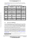
BR5 PM5350 - ATM UNI Buffered
PPC
14600801 Base at 14600000, 8 bit port size, no parity, GPCM
on PPC bus.
OR5 FFFF8E36 32K Byte block size, delayed CS assertion, early
CS and WE negation for write cycle, relaxed
timing, 7 w.s. for read, 8 for write, extended hold
time after read.
BR6 User’s peripheral Buffered
PPC
--
OR6 - -
BR7 User’s peripheral Buffered
PPC
--
OR7 - -
BR10 DSPRAM Local PPC 020000C1 Base at 200000, 64 bit port size, no parity,UPMC
OR10 FFF80000 512K Byte block size
BR11 DSP Peripherals Local PPC 01F00021 Base at 1F00000, 64 bit port size, no parity, GPCM
on local PPC bus.
OR11 FFFF0000 64K Byte block size
PSDMR SDRAM 64bit Non-buffered
PPC
C26B36A3
(C2692452)
Page interleaving, Refresh enabled, normal
operation, address muxing mode SDAM=2, A(15-
17) on BNKSEL(0:2), A8 on PSDA10, 8(4) clocks
refresh recovery, 3(2) clocks precharge to activate
delay, 3(2) clocks activate to read/write delay, 4
beat burst length, 2(1) clock last data out to
precharge, 2(1) clock write recovery time, Internal
address muxing, normal timing, 3(2) clocks CAS
latency.
SDRAM 32bit Non-buffered
PPC with
Host support
C28737A3
(C2432552)
Page interleaving, Refresh enabled, normal
operation, address muxing mode 1, A(13-15) on
BNKSEL(0:2), A9 on PSDA10, 8(4) clocks refresh
recovery, 3(2) clocks precharge to activate delay,
3(2) clocks activate to read/write delay, 8 beat
burst length, 2(1) clock last data out to precharge,
2(1) clock write recovery time, Internal address
muxing, normal timing, 3(2) clocks CAS latency.
PSRT SDRAM Supported
All PPC Bus
Config.
22 Generates refresh every 14 µsec, while 15.6 µsec
required. Therefore is refresh redundancy of 6.6
msec throughout full SDRAM refresh cycle which
completes in 64 msec. I.e., Application s/w may
withhold the bus upto app. 6.6 msec in a 57.3
msec period, without jeopardizing the contents of
the PPC bus SDRAM.
MPTPR SDRAM Supported 2800(1300) Divide Bus clock by 40D (20D)
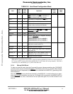
TABLE 4-4. Memory Controller Initialization for 100(50)
a
MHz
Reg. Device Type Bus
Init Value
[hex]
Description
Frees
cale Semiconductor,
I
Freescale Semiconductor, Inc.
For More Information On This Product,
Go to: www.freescale.com
nc...