


46 MSC8101ADS RevB User’s Manual MOTOROLA
Functional Description
5•6•2 SDRAM Refresh
The SDRAM is refreshed using its auto-refresh mode. I.e., using SDRAM machine 1’s periodic
timer, an auto-refresh command is issued to the SDRAM every 14 µsec, so that all 4096
A
SDRAM
rows are refreshed within spec’d
57.3 msec, while leaving a 6.6msec interval of refresh redundancy
within that window, as a safety measure, covering for possible delays in bus availability for the
refresh controller.
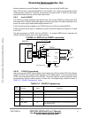
5•7 Flash Memory SIMM
The MSC8101 is provided with 8Mbyte of 90 nsec flash memory SIMM, the SM73228XG1JHBGO
by Smart Modular Technology which is composed of four LH28F016SCT-L95 chips by Sharp,
arranged as 2M X 32 in a single bank. Support is given also to 16MBytes and 32 MBytes Simm’s.
The Flash SIMM resides on an 80 pin SIMM socket and is buffered from the 60X bus to reduce
capacitive load over it.
To minimize use of MSC8101s’ chip-select lines, only one chip-select line CS0
is used to select
the Flash as a whole, while distributing chip-select lines among the module’s internal banks is done
by on-board programmable logic (BCSR), according to the Presence-Detect lines of the Flash
SIMM inserted to the MSC8101ADS.
The access time of the Flash memory provided with the MSC8101ADS is 95 nsec, however,
devices with different delay are supported as well. By reading the delay section of the Flash SIMM
Presence-Detect lines see TABLE 5-13. "Flash Presence Detect (7:5) Encoding" on page 59, the
debugger can establish via register OR0 the correct number of wait-states needed to access the
Flash SIMM (considering default system clock frequency).
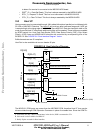
The control over the Flash is done with the GPCM and a dedicated CS0
region which controls the
whole bank. During hard - reset initialization
B
, the debugger or any application S/W for that matter,
reads the Flash Presence-Detect lines via BCSR and determines how to program registers BR0 &
OR0, within which the size and the delay of the region are determined. The performance of the
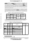
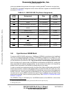
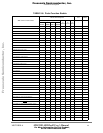
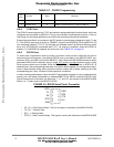
flash memory is shown in TABLE 5-5.:
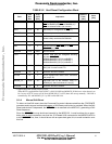
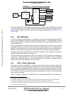
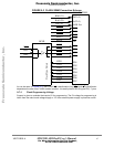
The Flash connection scheme is shown in FIGURE 5-3:
b. Two clocks latency setting is programmed for 50MHz Bus Clock
c. 8 beat burst is programmed for 32bit Data Bus width (Host Interface is active)
A. In fact each SDRAM component is composed of 4 internal banks each having 4096 rows, but they are re-
freshed in parallel.
B. i.e., initialization that follow the hard reset sequence at system boot.
TABLE 5-5. Flash Memory Projected Performance Figures
Number of System Clock Cycles
@ 100 MHz Bus Clock Freq.
Cycle Type \ Flash Delay [nsec] 95
Read Access
10
a
a. From TS asserted. However, due to internal activity, these figures may be larger.
Write
b
Access
b. The figures in the table refer to the actual write access. The write operation continues
internally and the device has to be polled for completion.
10
a
Frees
cale Semiconductor,
I
Freescale Semiconductor, Inc.
For More Information On This Product,
Go to: www.freescale.com
nc...