


42 MSC8101ADS RevB User’s Manual MOTOROLA
Functional Description
5•1•5 MSC8101 Internal Hard Reset Sources
The MSC8101 has internal sources which generate Hard / Soft Resets. Among these sources are:
1) Loss of Lock Reset (Hard)
2) S/W Watch Dog Reset (Hard)
3) Bus Monitor (Hard)
4) JTAG/ONCE Reset (Hard)
In general, the MSC8101 asserts a reset line HARD or SOFT for a period 512 clock cycles after
the reset source has been identified. A hard reset sequence is followed by a soft reset sequence
that released three bus clocks later than hard reset is negated.
5•2 Local Interrupter
There are external interrupts which are applied to the MSC8101ADS via its interrupt controller:
1) ABORT (NMI)
2) ATM UNI interrupt
5•2•1 ABORT Interrupt
The ABORT (NMI), is generated by a push-button. When this button is depressed, the IRQ0 input
to the MSC8101 is asserted. The purpose of this type of interrupt, is to support the use of resident
debugger if any is made available to the MSC8101ADS. To support external (off-board) generation
of an NMI, the IRQ0
line, is driven by an open-drain gate. This allows for an external h/w, to also
drive this line. If an external h/w indeed does so, it is compulsory that IRQ0
is driven by an open-
drain (or open-collector) gate.
5•2•2 ATM UNI Interrupt
To support ATM UNI (User Network I/F) event report by means of interrupt, the interrupt output of
the UNI (INTB) is connected to IRQ6
line of the MSC8101.
Since INTB of the UNI is an open-drain output, it is possible to connect additional (off-board) inter-
rupt requesters on the same IRQ6
, provided that they drive IRQ6 with open-drain gate as well.
5•2•3 QFALC Interrupt
Interrupt of T1/E1 Frame are served by IRQ7. The QFALC has an open-drain output, therefore it
is possible to connect additional (off-board) interrupt requesters on the IRQ7
line, the same way
as IRQ6
.
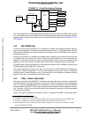
5•3 Clock Generator
The MSC8101 requires a single clock source for the main clock oscillator. Use is done with 25MHz
(16.38MHz) 3.3V clock generator mounted on the 14-pin DIP socket for simpler changing. Also
clock may be provided from external clock generator (reference) via SMB-connector. All MSC8101
PPC bus timings are referenced to the clock output of the DSP. The CLKOUT is connected to a
low inter-skew buffer to split the load between all various clock consumers on the board. One of
the channel intends for the MSC8101 DLL input to eliminate buffer and path propagation delay.
Special care is taken to isolate and terminate the clock route between the on-board devices and
the MSC8101, this to provide a "clean" clock for proper operation. The main clock scheme is
shown in figure below:
Frees
cale Semiconductor,
I
Freescale Semiconductor, Inc.
For More Information On This Product,
Go to: www.freescale.com
nc...