


MOTOROLA MSC8101ADS RevB User’s Manual 43
Functional Description
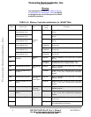
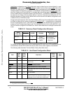
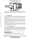
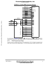
FIGURE 5-1 Clock Distribution Scheme
The Zero Delay Buffer CY2309 distributes high speed clock with skew less 250ps when internal
PLL is ON. Select inputs S1,S2 allow to the input clock be directly applied to the output with pro-
pogation delay of regular clock buffer about 5ns. See available working modes in TABLE 4-2. "JP1/
JP2 Settings".
5•4 Bus Buffering
In order to achieve best performance, it is necessary to reduce the capacitive load over the PPC
bus as much as possible. Therefore, the slower devices on the bus, i.e., the Flash SIMM, ATM UNI
M/P interface, BCSR and the external tool bus are buffered, while the SDRAM devices are not
buffered from the bus.
Buffers are provided over address and strobe (when necessary) lines while transceivers are
provided for data. Use is done with 74ALVT buffers (by Philips) which are 3.3V operated and 5V
tolerant
A
and provide bus hold to reduce pull-up/pull-down resistors count (as required by the
MSC8101). This type of buffers reduces noise on board due to reduced transition’s amplitude.
To further reduce noise and reflections, serial damping resistors may be added are placed over
SDRAM address and all MSC8101 strobe lines.
The data transceivers are open only if there is an access to a valid
B
buffered board address or
during Hard - Reset configuration
C
. That way data conflicts are avoided in case an unbuffered
memory read or off-board memory is read - provided that it is not mapped to an address valid on
board. It is the users’ responsibility to avoid such errors.
5•5 Chip - Select Generator
The memory controller of the MSC8101 is used as a chip-select generator to access on-board (and
off-board) memories, saving board’s area, reducing cost, power consumption and increasing flex-
ibility. To enhance off-board application development, memory modules (including the BCSRx)
may be disabled via BCSR
D
in favor of an external memory connected via the expansion connec-
tors. That way, a CS line may be used off-board via the expansion connectors, while its associated
local memory is disabled.
When a CS region, assigned to a buffered
E
memory, is disabled via BCSR, the local data trans-
A. Required for Flash SIMM and BCSR
B. An address which is covered in a Chip-Select region, that controls a buffered device by BCSR logic.
C. To allow a configuration word stored in the Flash memory or BCSR to become active.
D. After the BCSR is removed from the local memory map, there is no way to access it but to re-apply
power to the MSC8101ADS.
55MHz/
CLOCK OSC.
Zero
Delay
Buffer
SDRAM1
SDRAM2
BCSR
MICTOR
EXPANSION
CLKIN
MSC8101
CLKOUT
DLL_IN
A1
CY2309
20MHz
A2
A4
S2
S1
B1
B2
B3
JP2
VCC
VCC/
GND
U44
Frees
cale Semiconductor,
I
Freescale Semiconductor, Inc.
For More Information On This Product,
Go to: www.freescale.com
nc...