


B-90 MSC8101ADS RevB User’s Manual MOTOROLA
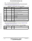
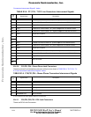
B•1•3 P3 - Altera’s In System Programming (ISP)
This is a 10 pin generic 0.100" pitch header connector, providing In System Programming capabil-
ity for Altera CPLD devices made programmable logic on board. The pinout of P3 is shown in
TABLE B1-4. "P3 - ISP Connector - Interconnect Signals" below:
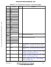
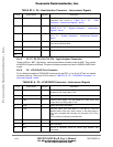
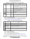
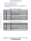
B•1•4 P4 - Host Interface Connector
This is a 36 pin two rows 0.100" pitch header connector. For more user’s convenience each of the
Host Interface signals is present at the CPM The pinout of P4 is shown in TABLE B1-5. "P4 - Host
Interface Connector - Interconnect Signals" below:
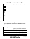
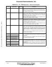
TABLE B1-4. P3 - ISP Connector - Interconnect Signals
Pin No. Signal Name Attribute Description
1 TCK I ISP Test port Clock. This clock shifts in / out data to / from the
programmable logic JTAG chain.
2 GND P Digital GND. Main GND plane.
3 TDO O ISP Transmit Data Output. This the prog. logic’s JTAG serial data
output driven by Falling edge of TCK.
4 VCC P Connect to 3.3V power supply bus for feeding an external
programmer logic.
5 TMS I ISP Test Mode Select. This signal qualified with TCK, changes
the state of the prog. logic JTAG machine.
6 N.C. - Not Connected.
7 N.C. - Not Connected.
8 N.C. - Not Connected.
9 TDI I ISP Transmit Data In. This is the prog. logic’s JTAG serial data
input, sampled by the MCS8101 on the rising edge of TCK.
10 GND P Digital GND. Main GND plane.
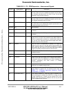
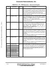
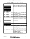
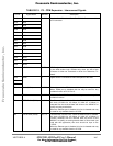
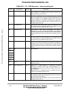
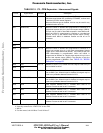
TABLE B1-5. P4 - Host Interface Connector - Interconnect Signals
Pin No. Signal Name Attribute Description
1 GND P Digital GND. Main GND plane.
2
Frees
cale Semiconductor,
I
Freescale Semiconductor, Inc.
For More Information On This Product,
Go to: www.freescale.com
nc...