


50 MSC8101ADS RevB User’s Manual MOTOROLA
Functional Description
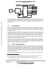
5•8•1 ATM Port
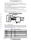
To support the MSC8101 ATM controller, a 155.52Mbps User Network Interface (UNI) is provided
on board, connected to FCC1 of the MSC8101 via UTOPIA I/F.Use is done with PM5350 S/UNI-
155-ULTRA by PMC-SIERA. Although these transceivers are capable of supporting 51.84Mbps
rate, support is given only to the higher rate.
The control over the transceiver is done using the microprocessor i/f of the transceiver, controlled
by the MSC8101 memory controller’s GPCM. Since the UNI is 5V powered and the MSC8101 3.3V
powered (5V intolerant), the UNI is buffered (LCX buffers) from the MSC8101 on both the receive
part of UTOPIA I/F and MP control ports.
The ATM transceiver may enabled / disabled at any time by writing ’0’ / ’1’ to the ATMEN~ bit in
BCSR1/2. When ATMEN~ is negated, (’1’) the MPcontrol port is also detached from the MSC8101
and its associated FCC1 may be used off-board via the expansion connectors.
The ATM transceiver reset input is driven by HRESET~ signal of the MSC8101, so that the UNI is
reset whenever a hard-reset sequence occurs. The UNI may also be reset by either asserting
ATM_RST bit in BCSR1/3 or by asserting (’1’) the RESET bit in the Master Reset and Identify /
Load Meters register via the UNI MP I/F.
The UNI transmit and receive clocks is fed with a 19.44 MHz +/- 20 ppm, clock generator, 5 V
powered, while the receive and transmit FIFOs’ clock is provided by the MSC8101, optionally from
the same clock or separate clocks, hard-configured.
The ATM SAR is connected to the physical medium by an optical I/F. Use is done with HP’s HFBR
5205 optical I/F, which operates at 1300 nm with upto 2 Km transmission range.
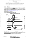
5•8•2 100/10 Base - T Port
A Fast Ethernet port with T.P. (100-Base-TX) I/F is provided on the MSC8101ADS. This port is
also support 10 Mbps ethernet (10-Base-T) via the same transceiver - the LXT970 by Level One.
The LXT970 is connected to FCC2 of the MSC8101 via MII interface, which is used for both -
device’s control and data path. The initial configuration of the LXT970 is done be setting desired
values at 8 configuration signals: FDE, CFG(0:1) and MF(0:4). The MF(0:4) pins however, are con-
trolled by 4 - voltage levels, this to allow each pin to configure two functions. On the MSC8101ADS
these pins is driven by factory set 0Ω resistors, connected to a voltage divider, allowing future
option change during production.
The LXT970 reset input is driven by HRESET~ signal of the MSC8101, resetting the transceiver
whenever hard-reset sequence is taken. The LXT970 may also be reset by either asserting the
FETH_RST bit in BCSR1/5 or by asserting bit 0.15 (MSB of LXT970 control register) via MII I/F.
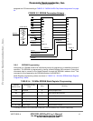
To allow external use of FCC2, its pins is appear at the CPM expansion connectors and the
PC30/TDMA1-TXCLK(CLK2)
+
PC31/TDMA1-RXCLK(CLK1)
+++
D
PD30/IDMA2-DRACK/IDMA2-DONE
+
PD31/IDMA1-DRACK/IDMA1-DONE
+
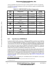
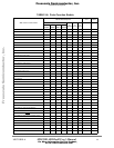
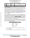
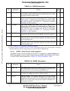
TABLE 5-6. Ports Function Enable
MSC8101 I/O Ports/Name
ADS On-Board Peripherals
DMA Ext.
Tool
Possible
Collision
QFALC on
CODEC
on
TDMA1
Fast Et
on
FCC2
ATM8
on
FCC1
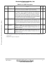
--
T1/E1
TDMA1
T1/E1
TDMB2
T1/E1
TDMC2
T1/E1
TDMD2
Frees
cale Semiconductor,
I
Freescale Semiconductor, Inc.
For More Information On This Product,
Go to: www.freescale.com
nc...