


MOTOROLA MSC8101ADS RevB User’s Manual 45
Functional Description
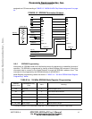
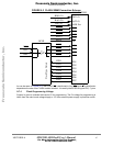
assigned to a CS line according to TABLE 5-3. "MSC8101ADS Chip Select Assignments" on page
44.
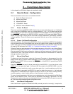
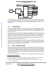
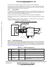
FIGURE 5-2 SDRAM Connection Scheme
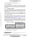
5•6•1 SDRAM Programming
After power-up, SDRAM needs to be initialized by means of programming, to establish its mode of
operation. The SDRAM is programmed by issuing a Mode Register Set command. During that
command data is passed to the Mode Register through the SDRAM’s address lines. This
command is fully supported by the SDRAM machine of the MSC8101.
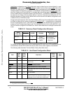
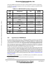
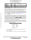
Mode Register programming values are shown in TABLE 5-4. "100 MHz SDRAM Mode Register
Programming" below:
TABLE 5-4. 100 MHz SDRAM Mode Register Programming
SDRAM
Address Line
a
a. Actually SDRAM’s A0 is connected to MSC8101 A29/A28 address line (32/64 bit width mode)
SDRAM Mode Reg
Field
Value Meaning:
A10 Reserved ‘0’ Should program zero
A9 WB ‘0’ Read & Write Burst Access
A8, A7 Operation Mode ‘00’ Standard Operation
A6 - A4 CAS Latency 3/2
b
CAS Latency
A3 Burst Type ‘0’ Sequential
A2 - A0 (LSB) Burst Length ’010’/’011’
c
4/8 Word Burst Length
CS
RAS
CAS
W
BA1
BA0
A(9:0)
CKE
CLK
DQM(0:3)
DQ(31:0)
CS
RAS
CAS
W
BA1
BA0
A(9:0)
CKE
CLK
DQM(0:3)
DQ(31:0)
CS2
RAS
CAS
WE
BNK0
SYSCLK1
D(0:31)
D(32:63)
DQM(0:3)
DQM(4:7)
A(0:9)
BNK1
MT48LC2M32B2 x 2
SDRAMEN64/32
A10 A10
PSDA10
A(29:19)
SYSCLK2
3.3
Address MUX
A29
A28
A27
A26
A0
A1
A2
A3
A19
A9
A20
32
64
Frees
cale Semiconductor,
I
Freescale Semiconductor, Inc.
For More Information On This Product,
Go to: www.freescale.com
nc...