


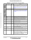
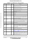

MOTOROLA MSC8101ADS RevB User’s Manual B-87
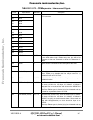
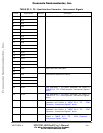
C15 HD0 I/O, T.S. Host Interface Bidirectional Data Port D0-D13. Present as well as
at P4 connector.
C16 HD1
C17 HD2
C18 HD3
C19 HD4
C20 HD5
C21 HD6
C22 HD7
C23 HD8
C24 HD9
C25 HD10
C26 HD11
C27 HD12
C28 HD13
C29 ATMRCLK O, T.S. ATM Receive Clock. A divide by 8 of the ATM line clock recovered
by the ATM receive logic. Enabled only when pin A29 of this
connector is either not connected or driven low. Otherwise, Tri-
stated.
C30 GND P Digital Ground. Connected to main GND plane of the ADS.
C31
C32
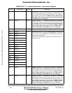
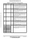
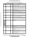
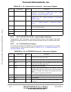
D1 CLK1(PC31) I/O, T.S. Clock 1 input. When TDMA is enabled this pin is an input clock.
When TDMA port is disabled this line may be used for any
available function of PC31 Port C.
D2 PC30 I/O, T.S. MSC8101’s Port C30 Parallel I/O line. May be used to any of its
available functions.
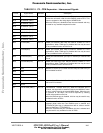
D3 FETHRXCK (PC29) I/O, T.S. Fast-Ethernet Receive Clock. When the Ethernet port is enabled,
this clock (25 MHz for 100 Mbps, 2.5 MHz for 10 Mbps) is
extracted from the received data and driven to the MSC8101 to
qualify incoming receive data.
When the Ethernet port is disabled, this line is tristated and may
be used for any available function of PC29.
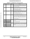
D4 FETHTXCK (PC28) I/O, T.S. Fast-Ethernet Transmit Clock. When the Ethernet port is enabled,
this clock (25 MHz for 100 Mbps, 2.5 MHz for 10 Mbps) is
normally extracted from the received data and driven to the
MSC8101 to qualify out coming transmit data. In Slave mode (not
used with this application) this clock should be input to the
LXT970.
When the Ethernet port is disabled, this line is tristated and may
be used for any available function of PC28.
TABLE B1-3. P2 - CPM Expansion - Interconnect Signals
Pin No. Signal Name Attribute Description
Frees
cale Semiconductor,
I
Freescale Semiconductor, Inc.
For More Information On This Product,
Go to: www.freescale.com
nc...