Rev.2.00 Nov 28, 2005 page 110 of 378
REJ09B0124-0200
M16C/6N Group (M16C/6NK, M16C/6NM) 12. DMAC
Under development
This document is under development and its contents are subject to change.
12.2 DMA Transfer Cycles
Any combination of even or odd transfer read and write addresses is possible.
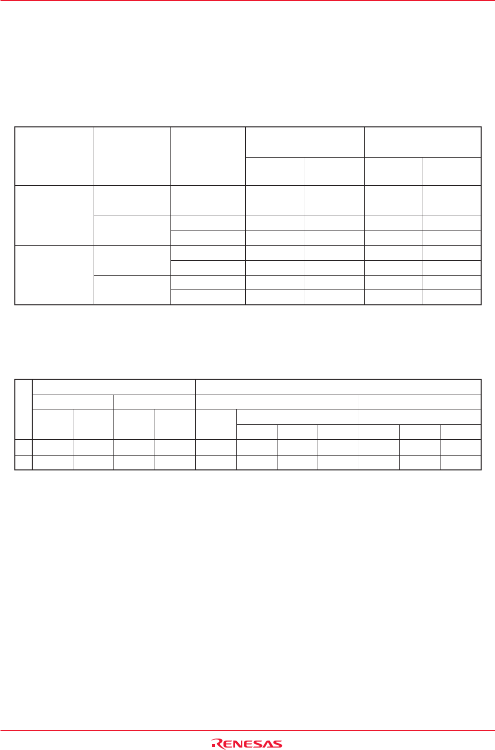
Table 12.2 shows the number of DMA transfer cycles. Table 12.3 shows the coefficient j, k.
The number of DMAC transfer cycles can be calculated as follows:
No. of transfer cycles per transfer unit = No. of read cycles ✕ j + No. of write cycles ✕ k
Table 12.2 DMA Transfer Cycles
NOTES:
1. Depends on the set value of the PM20 bit in the PM2 register.
2. Depends on the set value of the CSE register.
3. Not available external area in T/V-ver..
-
: This condition does not exist.
NOTE:
1. Not available memory expansion and microprocessor modes in T/V-ver..
Table 12.3 Coefficient j, k
Single-chip Mode
Memory Expansion Mode
Transfer Unit Bus Width Access Address
Microprocessor Mode
(1)
No. of Read No. of Write No. of Read No. of Write
Cycles Cycles Cycles Cycles
16 bits Even 1111
8-bit Transfer (BYTE = L) Odd 1111
(DMBIT =1) 8 bits Even
--
11
(BYTE= H) Odd
-
-11
16 bits Even 1111
16-bit Transfer (BYTE =L) Odd 2222
(DMBIT = 0) 8 bits Even
--
22
(BYTE = H) Odd
--
22
Internal Area External Area
(3)
Internal ROM, RAM
SFR Separate Bus Multiplexed Bus
No Wait
With Wait 1 Wait
(1)
2 Waits
(1)
No Wait
With Wait
(2)
With Wait
(2)
1 Wait 2 Waits 3 Waits 1 Wait 2 Waits 3 Waits
j12231234334
k12232234334
