Rev.2.00 Nov 28, 2005 page 49 of 378
REJ09B0124-0200
M16C/6N Group (M16C/6NK, M16C/6NM) 7. Bus
Under development
This document is under development and its contents are subject to change.
________
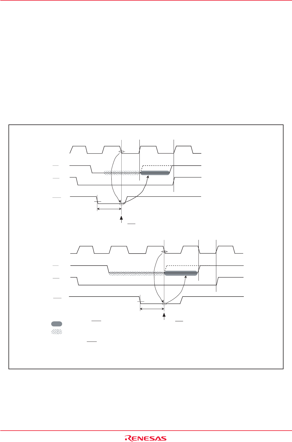
Figure 7.4 Example in which Wait State was Inserted into Read Cycle by RDY Signal
BCLK
RD
CSi
(i=0 to 3)
RDY
tsu(RDY - BCLK)
BCLK
RD
CSi
(i=0 to 3)
tsu(RDY - BCLK)
In an instance of separate bus
In an instance of multiplexed bus
Accept timing of RDY signal
: Wait using RDY signal
: Wait using software
Accept timing of RDY signal
tsu(RDY-BCLK): RDY input setup time
Shown above is the case where CSEi1W to CSEi0W (i = 0 to 3) bits in the CSE register are
"00b" (one wait state).
RDY
________
7.2.6 RDY Signal
This signal is provided for accessing external devices which need to be accessed at low speed. If input on
________
the RDY pin is asserted low at the last falling edge of BCLK of the bus cycle, one wait state is inserted in
________
the bus cycle. While in a wait state, the following signals retain the state in which they were when the RDY
signal was acknowledged.
_______ _______ _____ ________ ________ ______ ________ __________
A0 to A19, D0 to D15, CS0 to CS3, RD, WRL, WRH, WR, BHE, ALE, HLDA
________
Then, when the input on the RDY pin is detected high at the falling edge of BCLK, the remaining bus cycle
is executed. Figure 7.4 shows example in which the wait state was inserted into the read cycle by the
________ ________
RDY signal. To use the RDY signal, set the corresponding bit (CS3W to CS0W bits) in the CSR register
________ ________
to “0” (with wait state). When not using the RDY signal, the RDY pin must be pulled-up.


