Rev.2.00 Nov 28, 2005 page 46 of 378
REJ09B0124-0200
M16C/6N Group (M16C/6NK, M16C/6NM) 7. Bus
Under development
This document is under development and its contents are subject to change.
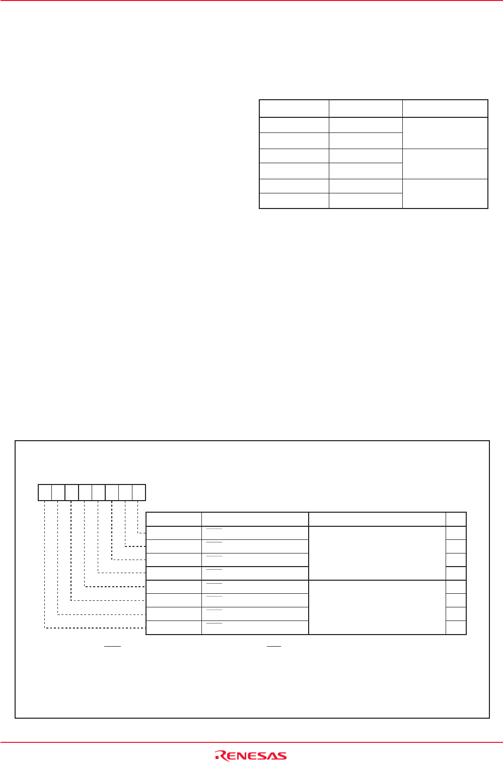
Figure 7.1 CSR Register
7.2 Bus Control
The following describes the signals needed for accessing external devices and the functionality of software
wait.
7.2.2 Data Bus
When input on the BYTE pin is high (data bus is an 8-bit width), 8 lines D0 to D7 comprise the data bus;
when input on the BYTE pin is low (data bus is a 16-bit width), 16 lines D0 to D15 comprise the data bus.
Do not change the input level on the BYTE pin while in operation.
7.2.3 Chip Select Signal
_____ ______
The chip select (hereafter referred to as the CS) signals are output from the CSi (i = 0 to 3) pins. These
_____
pins can be chosen to function as I/O ports or as CS by using the CSi bit in the CSR register.
Figure 7.1 shows the CSR register.
______
During 1 Mbyte mode, the external area can be separated into up to 4 by the CSi signal which is output
______
from the CSi pin.
______
Figure 7.2 shows the example of address bus and CSi signal output.
Set Value
(1)
Pin Function Address Bus Width
PM11 = 1 P3_4 to P3_7 12 bits
PM06 = 1 P4_0 to P4_3
PM11 = 0 A12 to A15 16 bits
PM06 = 1 P4_0 to P4_3
PM11 = 0 A12 to A15 20 bits
PM06 = 0 A16 to A19
NOTE:
1. No values other than those shown above can
be set.
7.2.1 Address Bus
The address bus consists of 20 lines, A0 to A19.
The address bus width can be chosen to be 12,
16 or 20 bits by using the PM06 bit in the PM0
register and the PM11 bit in the PM1 register.
Table 7.2 shows the PM06 and PM11 bits set
values and address bus widths.
When processor mode is changed from single-chip
mode to memory expansion mode, the address
bus is indeterminate until any external area is
accessed.
Table 7.2 PM06 and PM11 Bits Set Value and
Address Bus Width
0 : Chip select output disabled
(functions as I/O port)
1 : Chip select output enabled
0 : With wait state
1 : Without wait state
(1) (2) (3)
Chip Select Control Register
(4)
Symbol Address After Reset
Bit Name Function
Bit Symbol
NOTES:
1. Where the RDY signal is used in the area indicated by CSi (i = 0 to 3) or the multiplexed bus is used, set the
CSiW bit to "0" (Wait state).
2. If the PM17 bit in the PM1 register is set to "1" (with wait state), set the CSiW bit to "0" (with wait state).
3. When the CSiW bit = 0 (with wait state), the number of wait states (in terms of clock cycles) can be selected
using the CSEi1W to CSEi0W bits in the CSE register.
4. Not available this register in T/V-ver..
b7 b6 b5 b4 b3 b2 b1 b0
CSR 0008h 00000001b
CS3 Wait Bit
CS2 Wait Bit
CS1 Wait Bit
CS0 Wait Bit
CS3 Output Enable Bit
CS2 Output Enable Bit
CS0 Output Enable Bit
CS1 Output Enable Bit
RW
RW
RW
RW
RW
RW
RW
RW
RW
CS1
CS0
CS3
CS2
CS1W
CS0W
CS3W
CS2W


