Rev.2.00 Nov 28, 2005 page 263 of 378
REJ09B0124-0200
M16C/6N Group (M16C/6NK, M16C/6NM) 21. Flash Memory Version
Under development
This document is under development and its contents are subject to change.
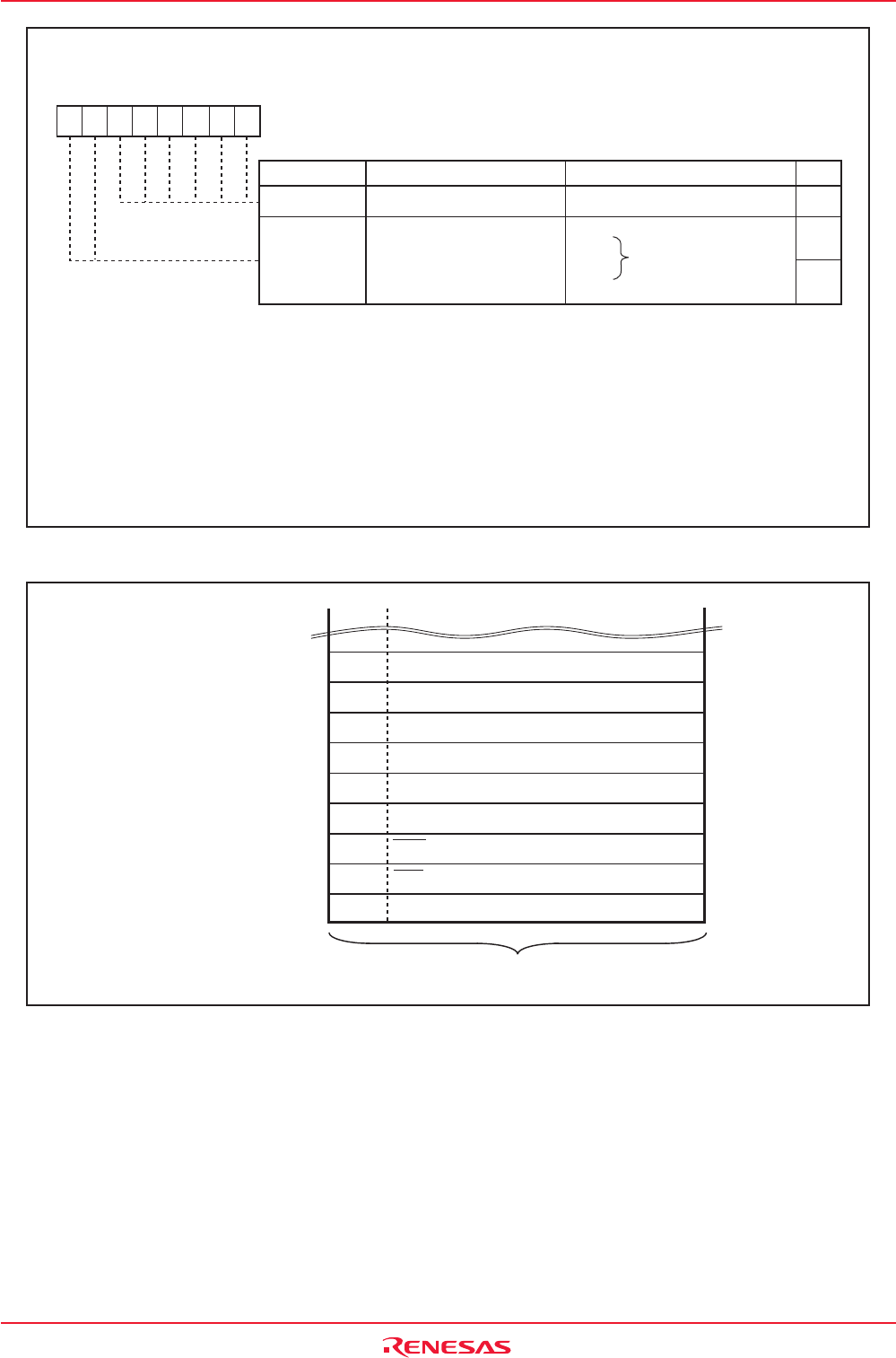
Figure 21.2 ROMCP Register
Figure 21.3 Address for ID Code Stored
ROM Code Protect Control Address
(5)
Symbol Address Value when Shipped
ROMCP 0FFFFFh FFh
(1)
b7 b6 b5 b4 b3 b2 b1 b0
1
Bit Symbol
Bit Name Function
Reserved Bit
ROM Code Protect Level 1
Set Bit
(1) (2) (3) (4)
Set to "1" RW
RW
RW
RW
-
(b5-b0)
ROMCP1
111 11
b7 b6
0 0 :
0 1 : Protect enabled
1 0 :
1 1 : Protect disabled
NOTES:
1. The ROMCP address is set to "FFh" when a block, including the ROMCP address, is erased.
2. When the ROM code protection is active by the ROMCP1 bit setting, the flash memory is protected against
reading or rewriting in parallel I/O mode.
3. Set the bit 5 to bit 0 to "111111b" when the ROMCP1 bit is set to a value other than "11b".
If the bit 5 to bit 0 are set to values other than "111111b", the ROM code protection may not become active
by setting the ROMCP1 bit to a value other than "11b".
4. To make the ROM code protection inactive, erase a block including the ROMCP address in CPU rewrite
mode, standard serial I/O mode or CAN I/O mode.
5. When a value of the ROMCPaddress is "00h" or "FFh", the ROM code protect function is disabled.
0FFFDFh to 0FFFDCh
0FFFE3h to 0FFFE0h
0FFFE7h to 0FFFE4h
0FFFEBh to 0FFFE8h
0FFFEFh to 0FFFECh
0FFFF3h to 0FFFF0h
0FFFF7h to 0FFFF4h
0FFFFBh to 0FFFF8h
0FFFFFh to 0FFFFCh
Reset vector
Oscillation stop and re-oscillation detection/Watchdog timer vector
Single step vector
Address match vector
BRK instruction vector
Overflow vector
Undefined instruction vector
NMI vector
DBC vector
ID7
ROMCP
ID6
ID5
ID4
ID3
ID2
ID1
Address
4 bytes


