Rev.2.00 Nov 28, 2005 page 59 of 378
REJ09B0124-0200
M16C/6N Group (M16C/6NK, M16C/6NM) 8. Clock Generating Circuit
Under development
This document is under development and its contents are subject to change.
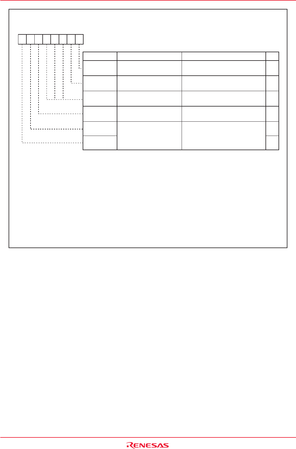
Figure 8.3 CM1 Register
RW
RW
RW
RW
RW
RW
RW
Bit Name FunctionBit Symbol
CM10
CM15
CM16
CM17
CM11
-
(b4-b2)
All Clock Stop Control
Bit
(2) (3)
XIN-XOUT Drive Capacity
Select Bit
(6)
Reserved Bit
Main Clock Division
Select Bit 1
(7)
System Clock Select Bit 1
(4)
0 : Clock on
1 : All clocks off (stop mode)
0 : LOW
1 : HIGH
Set to "0"
0 0 : No division mode
0 1 : Divide-by-2 mode
1 0 : Divide-by-4 mode
1 1 : Divide-by-16 mode
b7 b6
0 : Main clock
1 : PLL clock
(5)
Symbol
Address After Reset
CM1 0007h 00100000b
System Clock Control Register 1
(1)
000
b7 b6 b5 b4 b3 b2 b1 b0
NOTES:
1. Write to this register after setting the PRC0 bit in the PRCR register to "1" (write enable)
2. If the CM10 bit is "1" (stop mode), XOUT goes "H" and the internal feedback resistor is disconnected.
The XCIN and XCOUT pins are placed in the high-impedance state. When the CM11 bit is set to "1" (PLL
clock), or the CM20 bit in the CM2 register is set to "1" (oscillation stop, re-oscillation detection function enabled),
do not set the CM10 bit to "1".
3. When the PM22 bit in the PM2 register is set to "1" (watchdog timer count source is on-chip oscillator clock),
writing to the CM10 bit has no effect.
4. Effective when the CM07 bit is "0" and the CM21 bit is "0".
5. After setting the PLC07 bit in the PLC0 register to "1" (PLL operation), wait until tsu(PLL) elapses before
setting the CM11 bit to "1" (PLL clock).
6. When entering stop mode from high- or medium-speed mode, or when the CM05 bit is set to "1" (main clock
turned off) in low-speed mode, the CM15 bit is set to "1" (drive capability high).
7. Effective when the CM06 bit is "0" (CM16 and CM17 bits enabled).


