


RESETRESET and POWER-DOWN S3C9228/P9228
8-4
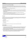
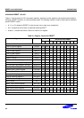
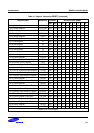
HARDWARE RESET RESET VALUES
Table 8-1 list the values for CPU and system registers, peripheral control registers, and peripheral data registers
following a RESET operation in normal operating mode. The following notation is used in these table to represent
specific RESET values:
— A "1" or a "0" shows the RESET bit value as logic one or logic zero, respectively.
— An 'x' means that the bit value is undefined following RESET.
— A dash ('–') means that the bit is either not used or not mapped.
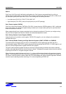
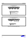
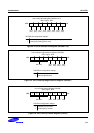
Table 8-1. Register Values after RESETRESET
Register Name Mnemonic Address
Bit Values after RESETRESET
Dec Hex 7 6 5 4 3 2 1 0
Locations B8H–B9H are not mapped.
Timer B Control Register TBCON 202 BAH – 0 0 0 0 0 0 –
Timer 1/A Control Register TACON 203 BBH 0 0 0 0 0 0 0 –
Timer B Data Register TBDATA 204 BCH 1 1 1 1 1 1 1 1
Timer A Data Register TADATA 205 BDH 1 1 1 1 1 1 1 1
Timer B Counter TBCNT 206 BEH 0 0 0 0 0 0 0 0
Timer A Counter TACNT 207 BFH 0 0 0 0 0 0 0 0
A/D Converter Control Register ADCON 208 D0H – – 0 0 0 0 0 0
A/D Converter Data Register (high byte) ADDATAH 209 D1H X X X X X X X X
A/D Converter Data Register (low byte) ADDATAL 210 D2H – – – – – – X X
Oscillator Control Register OSCCON 211 D3H – – – – 0 0 – 0
System Clock Control Register CLKCON 212 D4H 0 0 0 0 0 0 0 0
System Flags Register
FLAGS 213 D5H X X X X – – – –
Interrupt Pending Register 1
INTPND1 214 D6H 0 0 0 0 0 0 0 0
Interrupt Pending Register 2
INTPND2 215 D7H – – 0 0 0 0 0 0
LCD Port Control Register
LOPT 216 D8H – 0 0 0 0 0 0 0
Stack Pointer SP 217 D9H X X X X X X X X
Watch Timer Control Register WTCON 218 DAH 0 0 0 0 0 0 0 –
Locations DBH is not mapped.
Basic Timer Control Register BTCON 220 DCH 0 0 0 0 0 0 0 0
Basic Timer Counter BTCNT 221 DDH 0 0 0 0 0 0 0 0
Locations DEH is not mapped.