


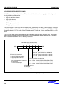


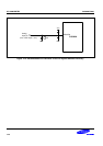

A/D CONVERTER S3C9228/P9228
14-2
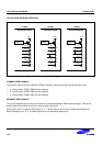
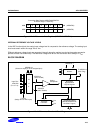
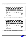
CONVERSION TIMING
The A/D conversion process requires 4 steps (4 clock edges) to convert each bit and 10 clocks to set-up A/D
conversion. Therefore, total of 50 clocks are required to complete an 10-bit conversion: When fxx/8 is selected
for conversion clock with an 4.5 MHz fxx clock frequency, one clock cycle is 1.78 us. Each bit conversion
requires 4 clocks, the conversion rate is calculated as follows:
4 clocks/bit × 10-bit + set-up time = 50 clocks, 50 clock × 1.78 us = 89 us at 0.56 MHz (4.5 MHz/8)
Note that A/D converter needs at least 25µs for conversion time.
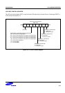
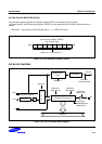
A/D CONVERTER CONTROL REGISTER (ADCON)
The A/D converter control register, ADCON, is located at address D0H in page 0. It has three functions:
— Analog input pin selection (bits 4 and 5)
— End-of-conversion status detection (bit 3)
— ADC clock selection (bits 2 and 1)
— A/D operation start or enable (bit 0 )
After a reset, the start bit is turned off. You can select only one analog input channel at a time. Other analog
input pins (AD0–AD3) can be selected dynamically by manipulating the ADCON.4–5 bits. And the pins not used
for analog input can be used for normal I/O function.
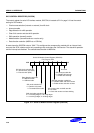
Start or enable bit
0 = Disable operation
1 = Start operation
(Automatically disable
the operation after
conversion completes.)
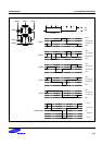
A/D Converter Control Register (ADCON)
D0H, Page0, R/W (EOC bit is read-only)
.7 .6 .5 .4 .3 .2 .1 .0MSB LSB
End-of-conversion bit
0 = Not complete Conversion
1 = complete Conversion
Always logic zero
A/D input pin selection bits:
00 = AD0
01 = AD1
10 = AD2
11 = AD3
Clock Selection bits:
00 = fxx/16
01 = fxx/8
10 = fxx/4
11 = fxx/1
Figure 14-1. A/D Converter Control Register (ADCON)