


S3C9228/P9228 A/D CONVERTER
14-3
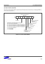
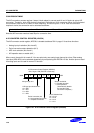
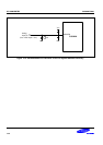
Conversion Data Register ADDATAH/ADDATAL
D1H/D2H, Page 0, Read Only
.9 .8 .7 .6 .5 .4 .3 .2MSB LSB (ADDATAH)
- - - - - - .1 .0MSB LSB (ADDATAL)
Figure 14-2. A/D Converter Data Register (ADDATAH/ADDATAL)
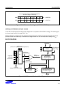
INTERNAL REFERENCE VOLTAGE LEVELS
In the ADC function block, the analog input voltage level is compared to the reference voltage. The analog input
level must remain within the range V
SS
to V
DD
.
Different reference voltage levels are generated internally along the resistor tree during the analog conversion
process for each conversion step. The reference voltage level for the first conversion bit is always 1/2 V
DD
.
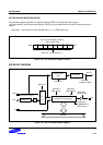
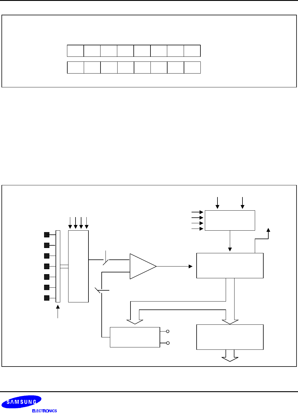
BLOCK DIAGRAM
Input Pins
AD0-AD3
(P1.0-P1.3)
Clock
Selector
Conversion Result
(ADDATAH/ADDATAL,
D1H/D2H, Page 0)
-
+
To ADCON.3
(EOC Flag)
Successive
Approximation
Logic & Register
VDD
VSS
Analog
Comparator
10-bit D/A
Converter
M
U
X
ADCON.4-5
(Select one input pin of the assigned pins)
P1CON
(Assign Pins to ADC Input)
ADCON.0
(AD/C Enable)
ADCON.0
(AD/C Enable)
.
.
.
ADCON.2-.1
Figure 14-3. A/D Converter Functional Block Diagram