


S3C9228/P9228 RESETRESET and POWER-DOWN
8-1
8 RESETRESET and POWER-DOWN
SYSTEM RESET
OVERVIEW
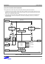
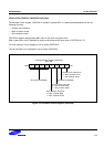
During a power-on reset, the voltage at V
DD
goes to High level and the RESET pin is forced to Low level. The
RESET signal is input through a schmitt trigger circuit where it is then synchronized with the CPU clock. This
procedure brings S3C9228/P9228 into a known operating status.
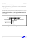
To allow time for internal CPU clock oscillation to stabilize, the RESET pin must be held to Low level for a
minimum time interval after the power supply comes within tolerance. The minimum required oscillation
stabilization time for a reset operation is 1 millisecond.
Whenever a reset occurs during normal operation (that is, when both V
DD
and RESET are High level), the
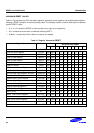
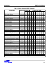
RESET pin is forced Low and the reset operation starts. All system and peripheral control registers are then reset
to their default hardware values (see Table 8-1).
In summary, the following sequence of events occurs during a reset operation:
— All interrupts are disabled.
— The watchdog function (basic timer) is enabled.
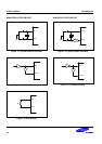
— The P0.0–P0.3, P1, and P2.2–P2.3 are set to schmitt trigger input mode and all pull-up resistors are disabled
for the I/O port pin circuits.
— Peripheral control and data registers are disabled and reset to their default hardware values.
— The program counter (PC) is loaded with the program reset address in the ROM, 0100H.
— When the programmed oscillation stabilization time interval has elapsed, the instruction stored in ROM
location 0100H (and 0101H) is fetched and executed.
NOTE
To program the duration of the oscillation stabilization interval, you make the appropriate settings to the
basic timer control register, BTCON, before entering Stop mode. Also, if you do not want to use the basic
timer watchdog function (which causes a system reset if a basic timer counter overflow occurs), you can
disable it by writing '1010B' to the upper nibble of BTCON.